To solve this problem, the QT1101 can also receive the ‘P’
character from the host on its ‘Rx’ pin separately from the
The spread-spectrum circuit can be eliminated if it is not
desired (see Section 3.1). Non spread-spectrum mode
1W pin (Figure 2.4). The host need not float the Rx line since consumes significantly less current in one of the LP modes.
the QT1101 will never try to drive it.
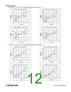
The spread-spectrum RC network might need to be modified
Following a ‘P’ on Rx, the QT1101 will send the same
slightly with longer burst lengths. The sawtooth waveform
response pattern (Figure 2.3) over the 1W line as in pure 1W observed on SS should reach a crest height as follows:
mode.
Vdd >= 3.6V: 17% of Vdd
All other comments and timings given for 1W operation are
applicable for 2W operation. LP operation is the same for
2W mode as for 1W.
Vdd < 3.6V: 20% of Vdd
The Css capacitor connected to SS (Figures 1.1 and 1.2)
should be adjusted so that the waveform approximates the
above amplitude, ±10%, during normal operation in the
target circuit. If this is done, the circuit will give a spectral
modulation of 12-15%.
If the Rx pin is not used, it must be tied to Vdd.
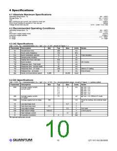
3 Design Notes
3.1 Oscillator Frequency
The QT1101’s internal oscillator runs from an external
network connected to the OSC and SS pins as shown in
Figures 1.1 and 1.2. The charts in these figures show the
recommended values to use depending on nominal
operating voltage and spread spectrum mode.
3.3 Cs Sample Capacitors - Sensitivity
The Cs sample capacitors accumulate the charge from the
key electrodes and determine sensitivity. Higher values of Cs
make the corresponding sensing channel more sensitive.
The values of Cs can differ for each channel, permitting
differences in sensitivity from key to key or to balance
unequal sensitivities. Unequal sensitivities can occur due to
key size and placement differences and stray wiring
capacitances. More stray capacitance on a sense trace will
desensitize the corresponding key; increasing the Cs for that
key will compensate for the loss of sensitivity.
If spread spectrum mode is not used, only resistor Rb1
should be used, the Css capacitor eliminated, and the SS
pin pulled to Vss with a 100K resistor.
The Cs capacitors can be virtually any plastic film or low to
medium-K ceramic capacitor. The ‘normal’ Cs range is 2 .2nF
to 50nF depending on the sensitivity required; larger values
of Cs require better quality to ensure reliable sensing.
Acceptable capacitor types for most uses include PPS film,
polypropylene film, and NP0 and X7R ceramics. Lower
grades than X7R are not advised.
An out-of-spec oscillator can induce timing problems such as
large variations in Max On-Duration times and response
times as well as on the serial port.
Effect on serial communications: The oscillator frequency
has no nominal effect on serial communications since the
baud rate is set by an auto-sensing mechanism. However, if
the oscillator is too far outside the recommended settings,
the possible range of serial communications can shrink. For
example, if the oscillator is too slow, the upper baud rate
range can be reduced.
The required values of Cs can be noticeably affected by the
presence and connection of the option resistors.
3.4 Power Supply
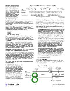
The burst pulses should always be in the range of 1.8-2.4µs
at the start of a burst to allow the serial port to operate at its
specified limits; in spread-spectrum mode, the first pulses of
a burst should ideally be 2.15µs. In non spread-spectrum
mode, the target value is 2µs. If in doubt, make the pulses
on the narrower side (i.e. a faster oscillator) when using the
higher baud rates, and conversely on the wider side when
using the lowest baud rates.
The power supply can range from 2.8V to 5.0V. If this
fluctuates slowly with temperature, the device will track and
compensate for these changes automatically with only minor
changes in sensitivity. If the supply voltage drifts or shifts
quickly, the drift compensation mechanism will not be able to
keep up, causing sensitivity anomalies or false detections.
The power supply should be locally regulated using a
three-terminal device, to between 2.8V and 5.0V. If the
supply is shared with another electronic system, care should
be taken to ensure that the supply is free of digital spikes,
sags, and surges which can cause adverse effects.
3.2 Spread Spectrum Circuit
The QT1101 offers the ability to spectrally spread its
frequency of operation to heavily reduce susceptibility to
external noise sources and to limit RF emissions. The SS pin
is used to modulate an external passive RC network that
modulates the OSC pin. OSC is the main oscillator current
input. The circuits and recommended values are shown in
Figures 1.1 and 1.2.
For proper operation a 0.1µF or greater bypass capacitor
must be used between Vdd and Vss. The bypass capacitor
should be routed with very short tracks to the device’s Vss
and Vdd pins.
The resistors Rb1 and Rb2 should be changed depending
on Vdd. As shown in Figures 1.1 and 1.2, three sets of
values are recommended for these resistors depending on
Vdd. The power curves in Section 4.6 also show the effect of
these resistors.
3.5 PCB Layout and Construction
Refer to Quantum application note AN-KD02 for information
related to layout and construction matters.
Lq
9
QT1101 R4.06/0806

 QUANTUM [ QUANTUM RESEARCH GROUP ]