T
M
Q U A L C O M M C D M A T E C H N O L O G I E S
HTTP://WWW.CDMATECH.COM
E N A B L I N G T H E F U T U R E O F C O M M U N I C A T I O N S
6
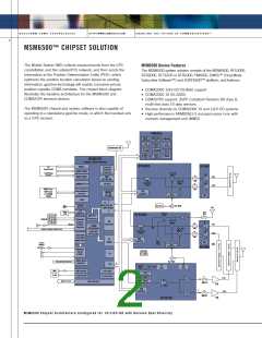
MSM6500™ CHIPSET SOLUTION
Included on the chip is the GPS LNA as well as the entire GPS VCO,
including resonant components. The Rx PLL, which resides on the
transmit companion chipset (the RFT6100 device), is switched
between the GPS Voltage Control Oscillator (VCO) and the external
Rx VCO.
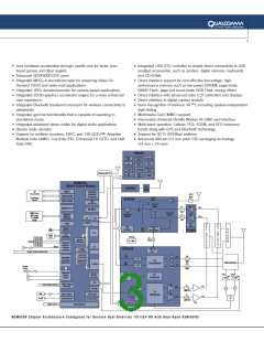
RFL6000 Device Description
Integrated into the RFL6000 device are two low-
noise amplifiers (LNAs): a cellular LNA and PCS
LNA. Both LNAs utilize three gain settings that
are programmable through the SBI.
Extension of standby time is achieved by selective circuit power
down, gain control and bias current. These features, along with all
radioOne chipset functions, are controlled by the MSM.
Operating modes—sleep, Rx, and Rx/Tx—as
well as LNA bias currents are all automatically adjusted via software
to minimize DC power consumption. Depending on handset status,
the LNA bias current adjusts to meet RF performance requirements
with minimal power consumption.
The RFR6000 device is designed to operate with 2.7 to 3.1 V power
supplies and is compatible with single-cell Li-Ion batteries.
Compatibility to the lower voltage (1.8 to 3.1 V) is assured when
VDDM is connected to the MSM pad voltage.
The RFL6000 device is fabricated using SiGe BiCMOS process,
which is suited for high performance RF circuits, and is packaged in
a very small 16-pin bump chip carrier (16-pin BCC++).
The RFR6000 chip is fabricated using a SiGe BiCMOS process,
which provides high-frequency, high-precision analog circuits as well
as low-power CMOS functions. Package type is 40 BCCP, which
includes a large ground slug for improved grounding, mechanical
strength and thermal conductivity.
RFL6000 Device Features
• Reduction in component count, space and cost via radioOne
chipset that eliminates receiver and transmitter IF
• Two integrated LNAs with programmable gain steps
• Cellular LNA supports CDMA and FM modes
– Cellular bands of operation in China, Japan, Korea, and the
United States
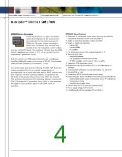
RFR6000 Device Features
• Compatibility with QCT’s radioOne Zero IF chipset that eliminates
the entire IF and reduces component count and space
• Single- or multi-band operation (cellular, PCS, GPS)
• Single- or multimode operation: cellular CDMA, PCS CDMA,
cellular FM and GPS
– Three CDMA gain settings
– Two FM gain settings
• PCS LNA supports PCS CDMA operation
– PCS bands of operation in China, Korea, and the United States
– Three CDMA gain settings
• Full downconversion—RF to baseband
• Receive path circuitry
• Programmable mode and bias control to reduce DC power
consumption
– GPS LNA
– Stepped gain control
• High reverse isolation
– Three-quadrature down converter
• Efficient three-line SBI
– Band-specific low-pass filter
• Low power consumption
• Baseband amplifiers with DC offset adjustment
• Need for only one single-band external VCO (Rx VCO) for all
CDMA bands of operation for entire radioOne chipset.
• Includes entire on-chip GPS VCO—including resonant circuit
• Individual circuit power on/off controls
• Power reduction feature control and extended handset standby
time
• Small package: 16-pin BCC++ (4 mm x 4 mm)
• SiGe BiCMOS process fabrication
RFR6000 Device Description
The RFR6000 device is the radioOne zero IF
downconverter. The device has three mixers
which, when combined with the RFL6000
device, provide full RF-to-baseband
– Selective circuit power-down
– Gain and bias controls
downconversion for the cellular, PCS and GPS
bands. The LO generation block produces all LO
signals, and only one external single-band VCO is required for all
CDMA frequency bands of operation.
• Low power supply voltage (2.7 to 3.1 V), low power dissipation
– Compatible with lower MSM voltage (1.8 to 3.0 Vdd)
• Small, thermally efficient package (40 BCC++)

 QUANTUM [ QUANTUM RESEARCH GROUP ]