5
• Efficient three-line SBI
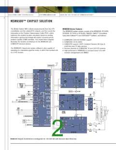
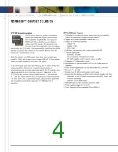
RTR6300 Device Description
• Power supply voltage (2.7 to 3.0 V)
• Small thermally efficient package (48-pin BCC++)
The RTR6300 device is a highly integrated RF
device that incorporates a dual-band CDMA 1X
transmitter with a dual-band GSM/GPRS
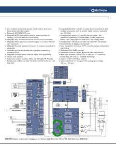
RTR6300 GSM/GPRS Transceiver Section
transceiver. It derives its architecture from QCT’s
radioOne direct conversion devices for CDMA.
The RTR6300 device also has an integrated transceiver for GSM
bands for both GSM and GPRS modes. It contains a dual-band
GSM/GPRS translational loop transmitter, which consists of lowpass
filtering with DC offset correction circuitry, I/Q modulators and offset
phase locked loop (OPLL). The transmit signals are derived from the
baseband interface from the MSM6500 device. The signals are
modulated to IF via the I/Q modulators, then applied to the OPLL
where its output drives the GSM Power Amplifier (PA). The GSM
receiver contains two LNAs, two direct conversion mixers and lowpass
filtering. Also on chip are two UHF PLLs designed to support fast
channel acquisition for GPRS and 3GPP compress mode operation.
RTR6300 CDMA 1X Transmit Section
The RTR6300 device contains all the upconversion and modulation
functionality necessary for CDMA and FM mode phones operating in
cellular and PCS bands. This transmit chip consists of two I/Q
modulators, one for cellular and one for the PCS band. The baseband
I/Q input from the MSM directly modulates the cellular or PCS carrier
derived from the respective LO generation circuit.
Both the cellular and PCS output drive their own VGA with a gain
control range of 85 dB. A final cellular driver amplifier provides a
modulated RF output. To accommodate split band and filtering, the
PCS VGA drives two output amplifiers that can be selected
independently or simultaneously via an input selectable switch. All RF
outputs have fully integrated 50-ohm matching networks.
The RTR6300 device voltage range is from 2.7 to 3.3 V, which
provides operating compatibility for platforms utilizing a single-cell Li-
Ion battery design. Operating modes for the RTR6300 device are
controlled by the MSM6500 chip via the three-line SBI, and include
selective power-down and gain control for optimal power savings and
talk-time improvement. The RTR6300 device is fabricated on an
Integrated on the RTR6300 device is the receiver PLL, transmit PLL
and the entire transmit VCO, including resonant components. The VCO
drives the LO generation block, which in turn generates the required
local oscillator signal for all CDMA bands of operation.
advanced SiGe BiCMOS process, which accommodates both precision
high-frequency analog circuits and low-power CMOS functions, and is
provided in a 48BCC++ plastic package that includes an exposed
center ground slug for improved RF grounding, mechanical strength
and thermal continuity.
RTR6300 CDMA 1X Transmit Features
• Reduction in component count, space and cost via radioOne
chipset that eliminates receiver and transmitter IF
• Single- or dual-band operation: cellular and PCS
• Single- or multimode operation:
RTR6300 GSM/GPRS Features
• Simple single-pole RC baseband reconstruction filter between
MSM6500 DAC and RTR6300 device
• Integrated synthesizer and LO generator system for GSM Tx/Rx and
CDMA 1X Tx bands, eliminating external RF components
– Two UHF PLLs designed to support Fast Channel Acquisition for
GPRS
– Cellular CDMA
– PCS CDMA
• Full direct upconversion from analog baseband to RF
• Transmit signal path:
• GSM receiver with settable gain states
– Baseband amplifier
• Integrated differential LNAs, mixers and baseband filter for receive
GSM operation
– Two-quadrature modulator/upconverter
– RF AGC amplifier, switch network, driver amplifier
• Integration of LO generation circuit
• Translational Loop Transmitter for GSM
– Need for second local oscillator eliminated
– Integrated low-pass filter and precision I/Q modulator
• Integrated DC auto-calibration system for GSM Tx/Rx operation
• MSM6500-controlled operation via newer, faster SBI
• Supply voltage from 2.7 to 3.3 V
• Requirement of only one external VCO for all CDMA bands of
operation
• Entire transmit synthesizer on chip (transmitter PLL and VCO)
• Receiver PLL on chip
• Greater than 85 dB transmit power control range
• Power reduction feature via MSM control extends handset talk time
– Optimized for low DC power consumption versus RF output level
– Transmit puncturing
• 48-pin BCC++ (7 x 7 mm2)
– Selective circuit power down

 QUANTUM [ QUANTUM RESEARCH GROUP ]