The QT114 is a digital burst mode charge-transfer (QT)
sensor designed specifically for point level sensing; it
includes all hardware and signal processing functions
necessary to provide stable level sensing under a wide
variety of changing conditions. Only a single external
capacitor is required for operation.
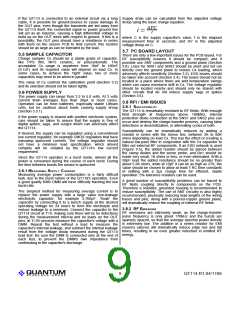
To 10x Scope Probe
Vcc
1
2MΩ
(optional)
2
3
4
7
6
OUT1 SNS2
OUT2 SNS1
OUT 1
OUT 2
To Electrode(s)
C
s
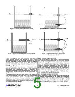
Figure 1-1 shows a basic QT114 circuit using the device, with
conventional OUT drives and power supply connections. The
sensing electrode can be connected to a single-tier or 2-tier
electrode as required.
1MΩ
multi-turn
pot (optional)
5
FILT
POL
Gnd
8
Calibration is done by design, through adjustment of the
electrode sizes and the Cs capacitor. Only under rare
situations do QT114 circuits require calibration on an
individual basis, and the circuit can make provision for that.
V
dd
V
dd
FILTER
POLARITY
POL: 1 = Active High
FILT: 1 = Slosh Filter
1 SIGNAL ACQUISITION
Figure 1-1 Standard mode options
The QT114 employs a short, low duty cycle burst of
charge-transfer cycles to acquire its signal. Burst mode
permits power consumption in the low microamp range,
dramatically reduces RF emissions, lowers susceptibility to
EMI, and yet permits excellent response time. Internally the
signals are digitally processed to generate the required
output signals.
It is not necessary to use both detection threshold points; if
only single point sensing is desired, only the lower threshold
and OUT1 can be used, while ignoring OUT2.
Two option pins allow the selection of output polarity and the
insertion of a 'slosh filter' before the OUT pins, as shown in
Figure 1-1.
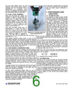
The QT switches and charge measurement hardware
functions are all internal to the QT114 (Figure 1-2). A 14-bit
single-slope switched capacitor ADC includes both the
required QT charge and transfer switches in a configuration
that provides direct ADC conversion. The burst length is
inversely proportional to the rate of charge buildup on Cs,
which in turn depends on the values of Cs, Cx, and Vcc. Vcc
is used as the charge reference voltage. Larger values of Cx
cause the charge transferred into Cs to accumulate more
rapidly. The trip points of the sensor can be changed by
altering Cs and Cx, the load capacitance. As a result, the
values of Cs, Cx, and Vcc should be fairly stable over the
expected operating temperature range.
1.1 ELECTRODE DRIVE
The internal ADC treats Cs as a floating transfer capacitor; as
a direct result, the sense electrode can be connected to
either SNS1 or SNS2 with no performance difference. The
polarity of the charge buildup across Cs during a burst is the
same in either case. Cs must be of within a certain range for
proper operation.
It is possible to connect separate Cx and Cx’ loads to SNS1
and SNS2 simultaneously, although the result is no different
than if the loads were connected together at SNS2 (or
SNS1). It is important to limit the amount of stray capacitance
on both terminals, especially if the load Cx is already large,
for example by minimizing trace lengths and widths so as not
to exceed the Cx load specification and to allow for a larger
sensing electrode size if so desired.
Two fixed thresholds are used, one for low fluid level and the
other for high level; adjusting Cs and Cx to allow these to trip
at appropriate points is required by design, and if required
may be trimmed by an adjustment. Figure 1-1 shows the
optional potentiometer which can be used to fine-tune the
placement of these threshold points relative to the signal.
The PCB traces, wiring, and any components associated with
or in contact with SNS1 and SNS2 will become proximity
sensitive and should be treated with caution.
1.2 THRESHOLD POINTS
The QT114 employs twin threshold points set at both
250 (for T1) and 150 counts (for T2) of acquisition
signal. The signal travels in an inverse direction:
increasing amounts of Cx reduce the signal level; the
baseline ('dry') signal should lie at 300 counts or more
under most conditions. Calibration details are
discussed fully in Section 3.2.
ELECTRODE
Result
SNS2
Cs
Start
Cx
2 ELECTRODE DESIGN
Done
The QT114 is designed to operate with a 'plateau'
sensor, having a substantial surface area at each
desired trip point, to create a capacitive 'step'.
SNS1
Charge
Amp
Figure 1-2 Internal Switching and Timing
LQ
2
QT114 R1.04/1106

 QUALCOMM [ QUALCOMM INCORPORATED ]