Preliminary Internet Data Sheet
HYI25DC512[16/80]0CE
512-Mbit Double-Data-Rate SDRAM
2
Chip Configuration
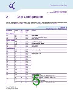
The chip configuration of a DDR SDRAM is listed by function in Table 3. The abbreviations used in the Pin#/Buffer# column
are explained in Table 4 and Table 5 respectively. The chip numbering for TSOP is depicted in Figure 1 .
TABLE 3
Chip Configuration of DDR SDRAM
Ball#/Pin#
Name
Pin
Type
Buffer
Type
Function
Clock Signals
45
CK
I
I
I
SSTL
SSTL
SSTL
Clock Signal
46
CK
Complementary Clock Signal
Clock Enable
44
CKE
Control Signals
23
22
21
24
RAS
CAS
WE
I
I
I
I
SSTL
SSTL
SSTL
SSTL
Row Address Strobe
Column Address Strobe
Write Enable
CS
Chip Select
Address Signals
26
27
29
30
31
32
35
36
37
38
39
40
28
BA0
I
I
I
I
I
I
I
I
I
I
I
I
I
I
I
I
SSTL
SSTL
SSTL
SSTL
SSTL
SSTL
SSTL
SSTL
SSTL
SSTL
SSTL
SSTL
SSTL
SSTL
SSTL
SSTL
Bank Address Bus 2:0
Address Bus 11:0
BA1
A0
A1
A2
A3
A4
A5
A6
A7
A8
A9
A10
AP
A11
A12
41
42
Address Signal 12
Note: Module based on 256 Mbit or larger dies
Note: Module based on 128 Mbit or smaller dies
Address Signal 13
NC
NC
I
—
17
A13
SSTL
Note: 1 Gbit based module
NC
NC
—
Note: Module based on 512 Mbit or smaller dies
Rev. 0.7, 2006-12
5
11292006-TAIE-H645

 QIMONDA [ QIMONDA AG ]