Preliminary Internet Data Sheet
HYI25DC512[16/80]0CE
512-Mbit Double-Data-Rate SDRAM
1
Overview
This chapter gives an overview of the 512-Mbit Double-Data-Rate SDRAM product family and describes its main
characteristics.
1.1
Features
•
Double data rate architecture: two data transfers per clock
cycle
Industrial operating temperature range: -40°C to +85°C
Bidirectional data strobe (DQS) is transmitted and
received with data, to be used in capturing data at the
receiver
DQS is edge-aligned with data for reads and is center-
aligned with data for writes
Differential clock inputs (CK and CK)
Four internal banks for concurrent operation
Data mask (DM) for write data
•
Commands entered on each positive CK edge; data and
data mask referenced to both edges of DQS
Burst Lengths: 2, 4, or 8
•
•
•
•
•
•
•
•
•
•
•
•
•
CAS Latency: 2, 2.5, 3
Auto Precharge option for each burst access
Auto Refresh and Self Refresh Modes
RAS-lockout supported tRAP = tRCD
7.8 µs Maximum Average Periodic Refresh Interval
2.5 V (SSTL_2 compatible) I/O
VDDQ = 2.5 V ± 0.2 V
VDD = 2.5 V ± 0.2 V
PG-TSOPII-66 package
RoHS Compliant Products
•
•
•
•
•
DLL aligns DQ and DQS transitions with CK transitions
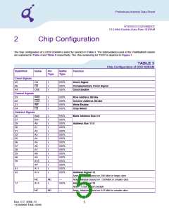
TABLE 1
Performance
Part Number Speed Code
–5
–6
Unit
Speed Grade
Component
@CL3
DDR400B
200
DDR333
166
—
Max. Clock Frequency
fCK3
MHz
MHz
MHz
@CL2.5
@CL2
fCK2.5
fCK2
166
166
133
133
Rev. 0.7, 2006-12
3
11292006-TAIE-H645

 QIMONDA [ QIMONDA AG ]