TOP252-262
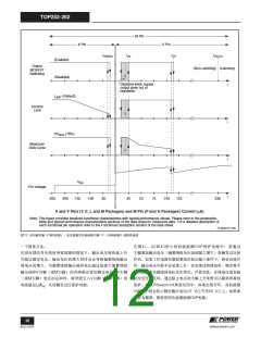
M Pin
X Pin
V Pin
IREM(N)
IUV
IOV
IOV(LS)
(Enabled)
Output
MOSFET
Switching
(Non-Latching) (Latching)
(Disabled)
Disabled when supply
output goes out of
regulation
I
ILIMIT (Default)
Current
Limit
I
DCMAX (78%)
Maximum
Duty Cycle
I
VBG
Pin Voltage
I
-250
-200
-150
-100
-50
0
25
50
75
100
125
336
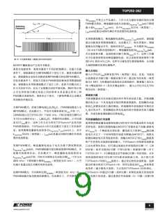
X and V Pins (Y, E, L and M Packages) and M Pin (P and G Packages) Current (µA)
Note: This figure provides idealized functional characteristics with typical performance values. Please refer to the parametric
table and typical performance characteristics sections of the data sheet for measured data. For a detailed description of
each functional pin operation refer to the Functional Description section of the data sheet.
PI-4646-071708
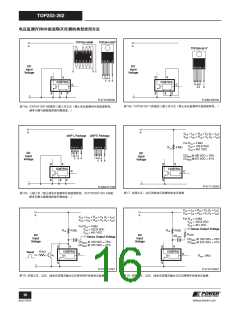
图 12. 多功能引脚(P和G封装)、电压监测及外部流限引脚(Y、E和M封装)的特性曲线
一个简单方法。
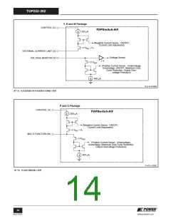
在图41、42和43所示的初级检测OVP保护电路中,是通过
大幅增加输出电压(偏置绕组电压因此随之增大)来触发过压保
护的。如果工作电源负载较重或在低压输入条件下,将会出现开
环,输出电压可能不会显著上升。在出现这些情况时,锁存将不
会关断直至负载或线电压发生变化。尽管如此,在线电压或负载
状况发生变化时,通过阻止电压的大幅上升依然可以提供所需的
保护。在TOPSwitch-HX典型应用中,如果出现开环,其初级侧
OVP保护将会阻止额定输出电压(12 V)上升至20 V之上。如果要
求更为精准,推荐使用次级侧检测OVP电路。
在因反馈信号失效而导致故障的情况下,输出电压将快速上升
并超过额定电压。输出电压的增大同时也会导致偏置绕组输出
端电压的增大。当偏置绕组输出端的电压超过连接于偏置绕组
输出端和V引脚(或M引脚)的齐纳稳压管的额定电压与V引脚
(或M引脚)电压的总和时,将导致引入V引脚(或M引脚)的
电流超过IV或IM,从而触发过压保护功能。
12
版本D 08/08
www.powerint.com

 POWERINT [ Power Integrations ]