TOP242-250
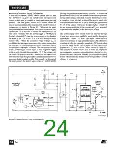
increase efficiency. This design delivers 70 W at 19 V, from an
85 VAC to 265 VAC input, at an ambient of 40 °C, in a small
sealed adapter case (4” x 2.15” x 1”). Full load efficiency is
85% at 85 VAC rising to 90% at 230 VAC input.
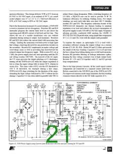
reduce Zener clamp dissipation. With a switching frequency of
132 kHz, a PQ26/20 core can be used to provide 70 W. To
maximize efficiency, by reducing winding losses, two output
windings are used each with their own dual 100 V Schottky
rectifier (D2 and D3). The frequency reduction feature of the
TOPSwitch-GX eliminates any dummy loading to maintain
regulation at no load and reduces the no-load consumption of
the power supply to only 520 mW at 230 VAC input. Frequency
jittering provides conducted EMI meeting the CISPR 22
(FCCB)/EN55022Bspecification,usingsimplefiltercomponents
(C7, L2, L3 and C6), even with the output earth grounded.
Duetothethermalenvironmentofasealedadapter, aTOP249Y
is used to minimize device dissipation. Resistors R9 and R10
externally program the current limit level to just above the
operating peak DRAIN current at full load and low line. This
allows the use of a smaller transformer core size without
saturation during startup or output load transients. Resistors
R9 and R10 also reduce the current limit with increasing line
voltage, limiting the maximum overload power at high input
line voltage, removing the need for any protection circuitry on
the secondary. Resistor R11 implements an under-voltage and
overvoltage sense as well as providing line feed-forward for
reduced output line frequency ripple. With resistor R11 set at
2 MΩ, the power supply does not start operating until the DC
rail voltage reaches 100 VDC. On removal of the AC input,
the UV sense prevents the output glitching as C1 discharges,
turning off the TOPSwitch-GX when the output regulation is
lost or when the input voltage falls to below 40 V, whichever
occurs first. This same value of R11 sets the OV threshold to
450 V. If exceeded, for example during a line surge,
TOPSwitch-GX stops switching for the duration of the surge,
extending the high voltage withstand to 700 V without device
damage. Capacitor C11 has been added in parallel with VR1 to
To regulate the output, an optocoupler (U2) is used with a
secondary reference sensing the output voltage via a resistor
divider (U3, R4, R5, R6). Diode D4 and C15 filter and smooth
the output of the bias winding. Capacitor C15 (1 µF) prevents
the bias voltage from falling during zero to full load transients.
Resistor R8 provides filtering of leakage inductance spikes,
keeping the bias voltage constant even at high output loads.
Resistor R7, C9 and C10 together with C5 and R3 provide
loop compensation.
Due to the large primary currents, all the small signal control
components are connected to a separate source node that is
Kelvin connected to the SOURCE pin of the TOPSwitch-GX.
Forimprovedcommon-modesurgeimmunity, thebiaswinding
common returns directly to the DC bulk capacitor (C1).
PERFORMANCE SUMMARY
D2
C7 2.2 nF
Y1 Safety
C13
0.33 µF 0.022 µF 0.01 µF
400 V 400 V 400 V
C12
C11
Output Power:
Regulation:
70 W
MBR20100
± 4%
Efficiency:
Ripple:
No Load Consumption:
≥ 84%
≤ 120 mV pk-pk
< 0.52 W @ 230 VAC
D3
MBR20100
VR1
P6KE-
200
C3
C14
19 V
@ 3.6 A
820 µF
0.1 µF
L1
200 µH
BR1
25 V
50 V
D1
RS805
UF4006
8A 600 V
C2
C4
RTN
820 µF
820 µF
R1
270 Ω
D4
1N4148
25 V
25 V
L2
820 µH
2A
R11
2 MΩ
1/2 W
R4
U2
31.6 kΩ
R8
4.7 Ω
PC817A
1%
C1
T1
R2
150 µF
C15
1 µF
50 V
R5
562 Ω
1%
1 kΩ
400 V
C6
TOPSwitch-GX
D
S
L
C9
0.1 µF
TOP249Y
L3
4.7 nF 50 V
X2
CONTROL
U1
75 µH
RT1
C
R9
2A
10 Ω
t°
13 MΩ
C10
1.7 A
R3
6.8 Ω
0.1 µF
R7
56 kΩ
X
F
F1
3.15 A
50 V
U3
TL431
C8
J1
R10
R6
4.75 kΩ
1%
0.1 µF
20.5 kΩ
C5
47 µF
16 V
L
50 V
All resistors 1/8 W 5% unless otherwise stated.
N
PI-2691-042203
Figure 42. 70 W Power Supply using Current Limit Reduction with Line and Line Sensing for UV and OV.
M
12/04
21

 POWERINT [ Power Integrations ]