TNY264/266-268
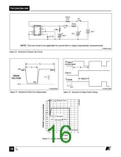
470 Ω
5 W
S2
470 Ω
EN/UV
S
D
S1
2 MΩ
S
S
S
50 V
10 V
BP
150 V
0.1 µF
NOTE: This test circuit is not applicable for current limit or output characteristic measurements.
PI-2686-101700
Figure 18. TinySwitch-II General Test Circuit.
DC
(internal signal)
MAX
t
2
t
t
P
1
HV
90%
90%
EN/UV
t
t
DRAIN
VOLTAGE
1
2
D =
t
EN/UV
V
DRAIN
10%
1
0 V
tP
=
fOSC
PI-2048-033001
PI-2364-012699
Figure 19. TinySwitch-II Duty Cycle Measurement.
Figure 20. TinySwitch-II Output Enable Timing.
t
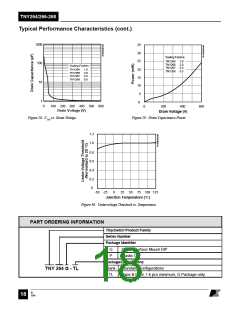
(Blanking Time)
LEB
1.3
1.2
1.1
1.0
0.9
0.8
0.7
0.6
0.5
0.4
0.3
0.2
0.1
0
I
INIT(MIN)
I
@ 100 °C
LIMIT(MIN)
0
1
2
3
4
5
6
7
8
Time (µs)
Figure 21. Current Limit Envelope.
B
7/01
16

 POWERINT [ Power Integrations ]