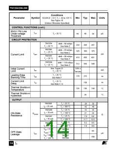
TNY264/266-268
Conditions
Parameter
Symbol SOURCE = 0 V; TJ = -40 to 125 °C
See Figure 18
Max
Units
Min
Typ
(Unless Otherwise Specified)
OUTPUT (cont.)
VBP = 6.2 V, VEN/UV = 0 V,
BVDSS
Breakdown
Voltage
V
700
IDS = 100 µA, TJ = 25 °C
tR
ns
ns
50
50
Rise Time
Fall Time
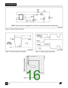
Measured in a Typical Flyback
Converter Application
tF
Drain Supply
Voltage
50
V
µs
µs
ms
%
Output EN/UV
Delay
tEN/UV
10
See Figure 20
Output Disable
Setup Time
0.5
tDST
TJ = 25 °C
See Note H
Auto-Restart
ON-Time
tAR
50
Auto-Restart
Duty Cycle
5.6
DCAR
NOTES:
A. Total current consumption is the sum of IS1 and IDSS when EN/UV pin is shorted to ground (MOSFET not switching)
and the sum of IS2 and IDSS when EN/UV pin is open (MOSFET switching).
B Since the output MOSFET is switching, it is difficult to isolate the switching current from the supply current at the
DRAIN. An alternative is to measure the BYPASS pin current at 6.1 V.
C. BYPASS pin is not intended for sourcing supply current to external circuitry.
D. See typical performance characteristics section for BYPASS pin start-up charging waveform.
E. For current limit at other di/dt values, refer to Figure 25.
F. This parameter is derived from characterization.
G. This parameter is derived from the change in current limit measured at 1X and 4X of the di/dt shown in the ILIMIT
specification.
H. Auto-restart on time has the same temperature characteristics as the oscillator (inversely proportional to
frequency).
B
7/01
15

 POWERINT [ Power Integrations ]