TNY263-268
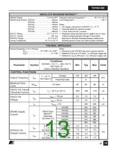
ABSOLUTE MAXIMUM RATINGS(1,4)
DRAIN Voltage ..................................................-0.3Vto700V Operating Junction Temperature(2) .................-40 °C to 150 °C
DRAIN Peak Current: TNY263......................................400mA Lead Temperature(3) ....................................................... 260 °C
TNY264......................................400mA
TNY265......................................440mA Notes:
TNY266......................................560mA 1. All voltages referenced to SOURCE, TA = 25 °C.
TNY267......................................720mA 2. Normally limited by internal circuitry.
TNY268......................................880mA 3. 1/16 in. from case for 5 seconds.
EN/UV Voltage ................................................ -0.3 V to 9 V 4. Maximum ratings specified may be applied one at a time,
EN/UV Current .................................................... 100 mA
BYPASS Voltage ..................................................-0.3 V to 9 V
Storage Temperature ......................................-65 °C to 150 °C
without causing permanent damage to the product.
Exposure to Absolute Maximum Rating conditions for
extended periods of time may affect product reliability.
THERMAL IMPEDANCE
Thermal Impedance: P or G Package:
Notes:
(θJA) ........................... 70 °C/W(2); 60 °C/W(3) 1. Measured on the SOURCE pin close to plastic interface.
(θJC)(1) ............................................... 11 °C/W 2. Soldered to 0.36 sq. in. (232 mm2), 2 oz. (610 g/m2) copper clad.
3. Soldered to 1 sq. in. (645 mm2), 2 oz. (610 g/m2) copper clad.
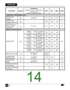
Conditions
SOURCE = 0 V; TJ = -40 to 125 °C
Parameter
Symbol
Min
Typ
Max
Units
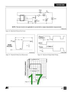
See Figure 18
(Unless Otherwise Specified)
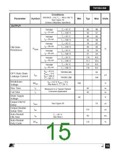
CONTROL FUNCTIONS
Average
124
132
8
140
TJ = 25 °C
See Figure 4
fOSC
kHz
Output Frequency
Peak-Peak Jitter
S1 Open
Maximum Duty
Cycle
DCMAX
62
65
68
%
EN/UV Pin Turnoff
Threshold Current
IDIS
TJ = -40 °C to 125 °C
-300
-240
-170
µA
IEN/UV = -125 µA
IEN/UV = 25 µA
VEN/UV = 0 V
0.4
1.3
1.0
2.3
1.5
2.7
EN/UV Pin
Voltage
VEN
V
IS1
430
500
µA
TNY263
200
225
245
265
315
380
250
270
295
320
380
460
TNY264
TNY265
TNY266
TNY267
TNY268
EN/UV Open
(MOSFET
Switching)
DRAIN Supply
Current
IS2
µA
See Note A, B
VBP = 0 V,
TJ = 25 °C
TNY263-264
TNY265-268
TNY263-264
TNY265-268
-5.5
-7.5
-3.8
-4.5
-3.3
-4.6
-2.0
-3.0
-1.8
-2.5
-1.0
-1.5
ICH1
See Note C, D
BYPASS Pin
Charge Current
mA
VBP = 4 V,
TJ = 25 °C
See Note C, D
ICH2
G
4/05
13

 POWERINT [ Power Integrations ]