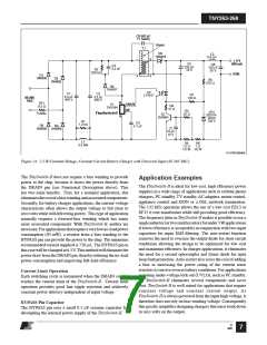
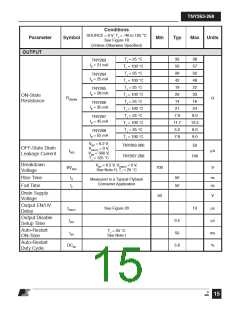
TNY263-268
2. A secondary output of 5 V with a Schottky rectifier diode.
Thermal Considerations
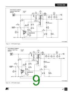
Copper underneath the TinySwitch-II acts not only as a single
point ground, but also as a heatsink. The hatched areas shown
in Figure 17 should be maximized for good heat sinking of
TinySwitch-II and the same applies to the output diode.
3. Assumed efficiency of 77% (TNY267 & TNY268),
75% (TNY265&TNY266)and73%(TNY263&TNY264).
4. The parts are board mounted with SOURCE pins soldered
to sufficient area of copper to keep the die temperature at
or below 100 °C.
EN/UV pin
If a line under-voltage detect resistor is used then the resistor
should be mounted as close as possible to the EN/UV pin to
minimize noise pick up.
In addition to the thermal environment (sealed enclosure,
ventilated, open frame, etc.), the maximum power capability
of TinySwitch-II in a given application depends on transformer
core size and design (continuous or discontinuous), efficiency,
minimum specified input voltage, input storage capacitance,
output voltage, output diode forward drop, etc., and can be
different from the values shown in Table 1.
Thevoltageratingofaresistorshouldbeconsideredfortheunder-
voltagedetect(Figure15:R2,R3)resistors. For1/4 Wresistors,
the voltage rating is typically 200 V continuous, whereas for
1/2 W resistors the rating is typically 400 V continuous.
Y-Capacitor
Audible Noise
The placement of the Y-capacitor should be directly from the
primary bulk capacitor positive rail to the common/return
terminal on the secondary side. Such placement will maximize
the EMI benefit of the Y-capacitor and avoid problems in
common-mode surge testing.
The TinySwitch-II practically eliminates any transformer audio
noiseusingsimpleordinaryvarnishedtransformerconstruction.
No gluing of the cores is needed. The audio noise reduction
is accomplished by the TinySwitch-II controller reducing the
current limit in discrete steps as the load is reduced. This
minimizes the flux density in the transformer when switching
at audio frequencies.
Optocoupler
It is important to maintain the minimum circuit path from
the optocoupler transistor to the TinySwitch-II EN/UV and
SOURCE pins to minimize noise coupling.
Worst Case EMI & Efficiency Measurement
Since identical TinySwitch-II supplies may operate at several
different frequencies under the same load and line conditions,
care must be taken to ensure that measurements are made under
worstcaseconditions.WhenmeasuringefficiencyorEMIverify
that the TinySwitch-II is operating at maximum frequency and
that measurements are made at both low and high line input
voltages to ensure the worst case result is obtained.
The EN/UV pin connection to the optocoupler should be kept
to an absolute minimum (less than 12.7 mm or 0.5 in.), and
this connection should be kept away from the DRAIN pin
(minimum of 5.1 mm or 0.2 in.).
Output Diode
Forbestperformance,theareaoftheloopconnectingthesecondary
winding, the output diode and the output filter capacitor, should
be minimized. See Figure 17 for optimized layout. In addition,
sufficient copper area should be provided at the anode and
cathode terminals of the diode for adequate heatsinking.
Layout
Single Point Grounding
Use a single point ground connection at the SOURCE pin for
the BYPASS pin capacitor and the Input Filter Capacitor
(see Figure 17).
Input and Output Filter Capacitors
There are constrictions in the traces connected to the input and
output filter capacitors. These constrictions are present for two
reasons. The first is to force all the high frequency currents
to flow through the capacitor (if the trace were wide then it
could flow around the capacitor). Secondly, the constrictions
minimizetheheattransferredfromtheTinySwitch-IItotheinput
filter capacitor and from the secondary diode to the output filter
capacitor. The common/return (the negative output terminal
in Figure 17) terminal of the output filter capacitor should be
connected with a short, low impedance path to the secondary
winding. In addition, the common/return output connection
should be taken directly from the secondary winding pin and
not from the Y-capacitor connection point.
Primary Loop Area
The area of the primary loop that connects the input filter
capacitor, transformer primary and TinySwitch-II together
should be kept as small as possible.
Primary Clamp Circuit
A clamp is used to limit peak voltage on the DRAIN pin at
turn-off. This can be achieved by using an RCD clamp (as
shown in Figure 14). A Zener and diode clamp (200 V) across
the primary or a single 550 V Zener clamp from DRAIN to
SOURCE can also be used. In all cases care should be taken
to minimize the circuit path from the clamp components to the
transformer and TinySwitch-II.
G
4/05
11

 POWERINT [ Power Integrations ]