TISPL758LF3D
INTEGRATED SYMMETRICAL AND ASYMMETRICAL BIDIRECTIONAL OVERVOLTAGE
PROTECTORS FOR LUCENT TECHNOLOGIES L7581/2/3 LINE CARD ACCESS SWITCHES
JANUARY 1998 - REVISED OCTOBER 1998
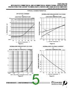
device to crowbar into a low-voltage on state. This low-voltage on state causes the current resulting from the
overvoltage to be safely diverted through the device. For negative surges, the high crowbar holding current
prevents d.c. latchup with the SLIC current, as the surge current subsides. The TISPL758LF3 is guaranteed
to voltage limit and withstand the listed international lightning surges in both polarities.
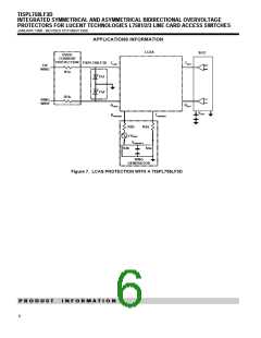
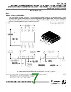
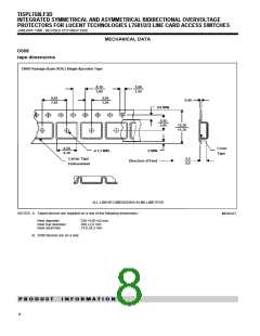
These protection devices are supplied in a small-outline surface mount (D) plastic package. The difference
between the TISPL758LF3D and TISPL758LF3DR versions is shown in the ordering information.
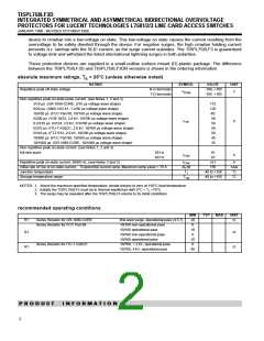
absolute maximum ratings, T = 25°C (unless otherwise noted)
A
RATING
SYMBOL
VALUE
UNIT
Repetitive peak off-state voltage
R-G terminals
-180, +105
-105, +105
VDRM
V
T-G terminals
Non-repetitive peak on-state pulse current (see Notes 1, 2 and 3)
2/10 µs (GR-1089-CORE, 2/10 µs voltage wave shape)
8/20 µs (ANSI C62.41, 1.2/50 µs voltage wave shape)
10/160 µs (FCC Part 68, 10/160 µs voltage wave shape)
5/200 µs (VDE 0433, 2.0 kV, 10/700 µs voltage wave shape)
0.2/310 µs (I3124, 2.0 kV, 0.5/700 µs voltage wave shape)
5/310 µs (ITU-T K20/21, 2.0 kV, 10/700 µs voltage wave shape)
5/310 µs (FTZ R12, 2.0 kV, 10/700 µs voltage wave shape)
10/560 µs (FCC Part 68, 10/560 µs voltage wave shape)
10/1000 µs (GR-1089-CORE, 10/1000 µs voltage wave shape)
Non-repetitive peak on-state current (see Notes 1, 2 and 3)
full sine wave
175
120
60
50
ITSP
A
50
50
50
45
35
50 Hz
60 Hz
16
20
ITSM
A
Repetitive peak on-state current, 50/60 Hz, (see Notes 2 and 3)
ITSM
diT/dt
TJ
2x1
A
A/µs
°C
Initial rate of rise of on-state current, Exponential current ramp, Maximum ramp value < 70 A
150
Junction temperature
-40 to +150
-40 to +150
Storage temperature range
Tstg
°C
NOTES: 1. Above the maximum specified temperature, derate linearly to zero at 150°C lead temperature.
2. Initially the TISPL758LF3 must be in thermal equilibrium with 0°C < TJ <70°C.
3. The surge may be repeated after the TISPL758LF3 returns to its initial conditions.
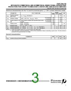
recommended operating conditions
MIN
20
0
TYP
MAX
UNIT
R1
R1
Series Resistor for GR-1089-CORE
Series Resistor for FCC Part 68
first-level surge, operational pass (4.5.7)
10/160 non-operational pass
10/160 operational pass
W
18
0
W
W
10/560 non-operational pass
10/560 operational pass
10
0
Series Resistor for ITU-T K20/21
10/700, < 2 kV, operational pass
10/700, 4 kV, operational pass
R1
40
P R O D U C T
I N F O R M A T I O N
2

 POINN [ POWER INNOVATIONS LTD ]