S/UNI®-ATLAS-3200 Telecom Standard Product Data Sheet
Preliminary
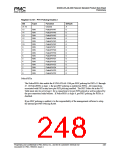
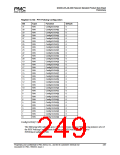
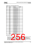
Register 0x144: PHY Policing RAM Address and Access Control
Bit
31:19
18
17
16
15
14
13
12
11
10
9
8
7
6
5
4
3
2
1
Type
Function
Unused
RWB
BUSY
Default
X
1
X
0
0
0
0
0
0
0
0
0
0
0
0
0
0
0
0
0
R/W
R
R/W
R/W
R/W
R/W
R/W
R/W
R/W
R/W
R/W
R/W
R/W
R/W
R/W
R/W
R/W
R/W
R/W
CLRONRD
Wr_PhyConfig
Wr_PhyNonComp3
Wr_PhyNonComp2
Wr_PhyNonComp1
Wr_Reserved
Wr_PHYI
Wr_PhyL
Wr_PhyTAT
Unused
Unused
PHYAddr[5]
PHYAddr[4]
PHYAddr[3]
PHYAddr[2]
PHYAddr[1]
PHYAddr[0]
0
PHYAddr[5:0]
The PHYAddr[5:0] bits indicate which of the per-PHY RAM locations is going to be
accessed. PHYAddr[5:0]=000000 holds the policing parameters and non-compliant cell
counts for PHY 1, and PHYAddr[5:0]=101111 holds the policing parameters and non-
compliant cell counts for PHY48.
Wr_PhyTAT
When Wr_PhyTAT is logic 1, then a write access to the PHY Policing RAM will write to the
PhyTAT field. When it is logic 0, the contents of PhyTAT will be unchanged after a write
access. These bits should be written to zero on setup and left alone thereafter.
Wr_PhyL
When Wr_PhyL is logic 1, then a write access to the PHY Policing RAM will write to the
PhyL field and the two Unused bits contiguous with it. When it is logic 0, the contents of
PhyL and the Unused bits will be unchanged after a write access.
Proprietary and Confidential to PMC-Sierra, Inc., and for its Customers’ Internal Use
Document ID: PMC-1990553, Issue 4
252

 PMC [ PMC-SIERRA, INC ]