(Preliminary)PL611s-27
1.8V to 3.3V PicoPLLTM Programmable Clock
KEY PROGRAMMING PARAMETERS
CLK
Programmable
Input/Output
Output Drive Strength
Output Frequency
F
OUT = FREF * M / (R * P)
Where M = 11 bit
R = 8 bit
Three optional drive strengths to
choose from:
One output pin can be configured
as:
P = 5 bit
• Low: 4mA
• OE - input
CLK0 = FOUT, FREF or FREF / (2*P)
CLK1 = FREF, FREF/2, CLK0 or CLK0/2
• Std: 8mA (default)
• High: 16mA
• PDB - input
• FSEL – input
•
HiZ or Active Low disabled state
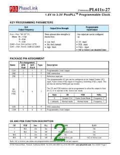
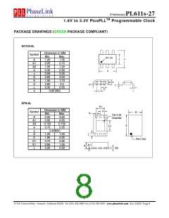
PACKAGE PIN ASSIGNMENT
Pin Assignment
Name
Type
Description
DFN
Pin#
SOT
Pin #
CLK1
GND
FIN
2
3
1
1
2
3
O
P
I
Programmable Clock Output
GND connection
Reference input pin
This programmable I/O pin can be configured as an Output Enable (OE)
input, Power Down (PDB) input or Frequency Switching (FSEL) input. This
pin has an internal 60KΩ pull up resistor.
The OE and PDB features can be programmed to allow the output to float
(Hi Z), or to operate in the ‘Active low’ mode.
OE,
PDB,
FSEL
6
4
I
State
OE
PDB
FSEL
0
Disable CLK
Normal mode
Power Down Mode
Normal mode
Frequency ‘2’
Frequency ‘1’
1 (default)
VDD
5
4
5
6
P
VDD connection
CLK0
O
Programmable Clock Output
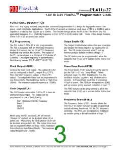
OE AND PDB FUNCTION DESCRIPTION
OE
PDB
Osc.
PLL
CLK0
CLK1
1
N/A
N/A
1
On
On
On
Off
On
Off
On
Off
On
On
On
On
0
HiZ or Active Low
On
N/A
N/A
0
HiZ or Active Low
HiZ or Active Low
Note: HiZ or Active Low states are programmable functions and will be set per request.
47745 Fremont Blvd., Fremont, California 94538 Tel (510) 492-0990 Fax (510) 492-0991 www.phaselink.com Rev 2/25/07 Page 2

 PLL [ PHASELINK CORPORATION ]