TDA8944J
2 x 7 W stereo BTL audio amplifier
Philips Semiconductors
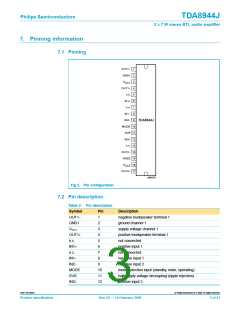
Table 3: Pin description…continued
Symbol
Pin
13
14
15
16
17
Description
n.c.
not connected
OUT2−
GND2
VCC2
negative loudspeaker terminal 2
ground channel 2
supply voltage channel 2
positive loudspeaker terminal 2
OUT2+
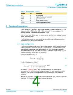
8. Functional description
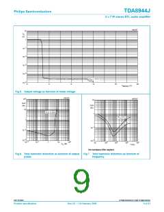
The TDA8944J is a stereo BTL audio power amplifier capable of delivering 2 × 7 W
output power to an 8 Ω load at THD = 10%, using a 12 V power supply and an
external heatsink. The voltage gain is fixed at 32 dB.
With the three-level MODE input the device can be switched from ‘standby’ to ‘mute’
and to ‘operating’ mode.
The TDA8944J outputs are protected by an internal thermal shutdown protection
mechanism and a short-circuit protection.
8.1 Input configuration
The TDA8944J inputs can be driven symmetrical (floating) as well as asymmetrical.
In the asymmetrical mode one input pin is connected via a capacitor to the signal
ground which should be as close as possible to the SVR (electrolytic) capacitor
ground. Note that the DC level of the input pins is half of the supply voltage VCC, so
coupling capacitors for both pins are necessary.
The input cut-off frequency is:
1
f i(cut – off )
=
(1)
(2)
------------------------------
2 – (Ri × Ci)
For Ri = 45 kΩ and Ci = 220 nF:
1
f i(cut – off )
=
= 16 Hz
------------------------------------------------------------------
2 – (45 × 103 × 220 × 10–9
)
As shown in Equation 1 and 2, large capacitor values for the inputs are not
necessary; so the switch-on delay during charging of the input capacitors, can be
minimized. This results in a good low frequency response and good switch-on
behaviour.
Remark: To prevent HF oscillations do not leave the inputs open, connect a capacitor
of at least 1.5 nF across the input pins close to the device.
9397 750 06861
© Philips Electronics N.V. 2000. All rights reserved.
Product specification
Rev. 02 — 14 February 2000
4 of 21

 NXP [ NXP ]