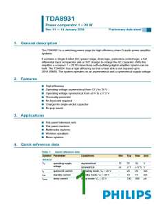
TDA8931
Philips Semiconductors
Power comparator 1 × 20 W
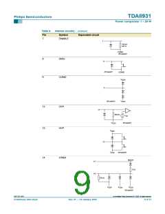
8. Functional description
8.1 General
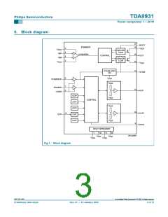
The TDA8931 is a switching power stage for high efficiency class-D audio power amplifier
systems. It contains a Single-Ended (SE) power stage, drive logic, protection control logic,
a full differential input comparator and a HVP charger to charge the SE capacitor (see
Figure 1). With this amplifier a compact 1 × 20 W closed loop self-oscillating digital
amplifier system can be built. A second order low-pass filter converts the PWM output
signal into an analog audio signal across the speaker.
8.2 Interfacing
The operating modes of the TDA8931 can be controlled by pins POWERUP and ENABLE.
Both pins refer to pin CGND. The device has three modes:
• Sleep mode
• Standby mode
• Operating mode
When pin POWERUP = LOW, the power comparator is in Sleep mode, independent of the
signal on pin ENABLE. In Sleep mode the SE capacitor charger will be discharged.
When pin POWERUP = HIGH and pin ENABLE = LOW the device is in Standby mode. In
Standby mode the device is DC biased and the SE capacitor will be charged and the
output is floating.
When both pins POWERUP and ENABLE are HIGH, the device is in Operating mode. A
level at pin POWERUP greater than 11 V can also enter the Operating mode, independent
of the level on pin ENABLE (see Table 4).
Remark: The switch-on sequence is important. First pin POWERUP = HIGH, then pin
ENABLE = HIGH.
Table 4:
Interfacing
Voltage on pin
POWERUP
< 0.8 V
Mode
ENABLE
-
Sleep
3 V to 7 V
< 0.8 V
> 3 V
-
Standby
Operating
Operating
> 11 V
8.3 Input comparator
The input comparator has a full differential input and is optimized for low noise and low
offset. This results in maximum flexibility in the application.
8.4 Half supply voltage input reference (pin HVPI)
When the device is in Standby mode, the external capacitor C6 (see Figure 5) will be
charged until it reaches the half of the supply voltage. This pin charges capacitor C6
within 0.5 seconds.
9397 750 13847
© Koninklijke Philips Electronics N.V. 2005. All rights reserved.
Preliminary data sheet
Rev. 01 — 14 January 2004
5 of 31

 NXP [ NXP ]