TDA8931
Philips Semiconductors
Power comparator 1 × 20 W
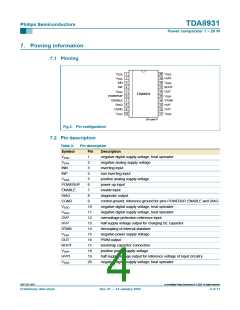
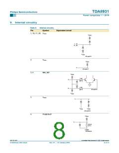
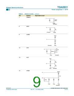
7. Pinning information
7.1 Pinning
1
2
20
19
18
17
16
15
14
13
12
11
V
V
SSD
SSD
V
HVPI
SSA
3
INN
V
DDP
4
INP
DDA
BOOT
OUT
5
V
TDA8931
6
POWERUP
ENABLE
DIAG
V
SSP
7
STABI
HVP
8
9
CGND
OVP
10
V
V
SSD
SSD
001aab811
Fig 2. Pin configuration
7.2 Pin description
Table 3:
Symbol
VSSD
Pin description
Pin
1
Description
negative digital supply voltage; heat spreader
negative analog supply voltage
inverting input
VSSA
2
INN
3
INP
4
non inverting input
VDDA
5
positive analog supply voltage
POWERUP
ENABLE
DIAG
CGND
VSSD
6
power-up input
7
enable input
8
diagnostic output
9
control ground; reference ground for pins POWERUP, ENABLE and DIAG
negative digital supply voltage; heat spreader
negative digital supply voltage; heat spreader
overvoltage protection reference input
half supply voltage output for charging SE capacitor
decoupling of internal stabilizer
negative power supply voltage
10
11
12
13
14
15
16
17
18
19
20
VSSD
OVP
HVP
STABI
VSSP
OUT
PWM output
BOOT
VDDP
bootstrap capacitor connection
positive power supply voltage
HVPI
half supply voltage output for reference voltage of input circuitry
negative digital supply voltage; heat spreader
VSSD
9397 750 13847
© Koninklijke Philips Electronics N.V. 2005. All rights reserved.
Preliminary data sheet
Rev. 01 — 14 January 2004
4 of 31

 NXP [ NXP ]