TDA8922B
Philips Semiconductors
2 × 50 W class-D power amplifier
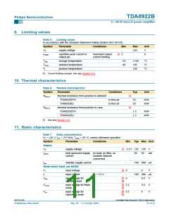
Table 7:
Static characteristics …continued
VP = ±26 V; fosc = 317 kHz; Tamb = 25 °C; unless otherwise specified.
Symbol Parameter Conditions
Audio inputs; pins IN1M, IN1P, IN2P and IN2M
VI DC input voltage
Amplifier outputs; pins OUT1 and OUT2
Min
Typ Max Unit
[2]
-
0
-
V
VOO(SE)(mute)
VOO(SE)(on)
VOO(BTL)(mute)
VOO(BTL)(on)
mute SE output offset
voltage
-
-
-
-
-
-
-
-
15
mV
[4]
[4]
operating SE output
offset voltage
150 mV
21 mV
210 mV
mute BTL output offset
voltage
operating BTL output
offset voltage
Stabilizer output; pin STABI
Vo(stab) stabilizer output
voltage
Temperature protection
Tprot temperatureprotection
mute and operating;
with respect to VSSP1
11
12.5 15
V
-
-
150
20
-
-
°C
°C
activation
Thys
hysteresis on
temperature protection
[1] The circuit is DC adjusted at VP = ±12.5 V to ±30 V.
[2] With respect to SGND (0 V).
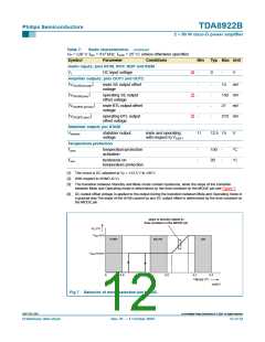
[3] The transition between Standby and Mute mode contain hysteresis, while the slope of the transition
between Mute and Operating mode is determined by the time-constant on the MODE pin see Figure 7.
[4] DC output offset voltage is applied to the output during the transition between Mute and Operating mode in
a gradual way.The slope of the dV/dt caused by any DC output offset is determined by the time-constant on
the MODE pin.
slope is directly related to
time-constant on the MODE pin
V
(V)
O
V
oo
(on)
STBY
MUTE
ON
V
(mute)
oo
0
0.8
2.2
3.0
4.2
5.5
V
MODE
(V)
coa021
Fig 7. Behavior of mode selection pin MODE.
9397 750 13357
© Koninklijke Philips Electronics N.V. 2004. All rights reserved.
Preliminary data sheet
Rev. 01 — 1 October 2004
12 of 32

 NXP [ NXP ]