TDA8920B
Philips Semiconductors
2 × 100 W class-D power amplifier
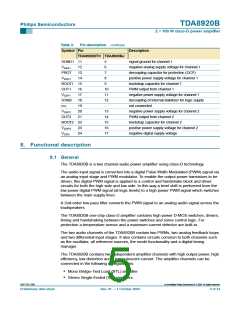
The amplifier system can be switched in three operating modes with pin MODE:
• Standby mode; with a very low supply current
• Mute mode; the amplifiers are operational; but the audio signal at the output is
suppressed by disabling the VI-converter input stages
• Operating mode; the amplifiers are fully operational with output signal.
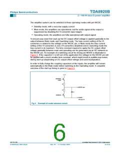
To ensure pop-noise free start-up the DC output offset voltage is applied gradually to the
output between Mute mode and Operating mode. The bias current setting of the VI
converters is related to the voltage on the MODE pin; in Mute mode the bias current
setting of the VI converters is zero (VI converters disabled) and in Operating mode the
bias current is at maximum. The time constant required to apply the DC output offset
voltage gradually between mute and operating can be generated via an RC-network on
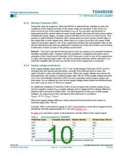
the MODE pin. An example of a switching circuit for driving pin MODE is illustrated in
Figure 4. If the capacitor C is left out of the application the voltage on the MODE pin will
be applied with a much smaller time-constant, which might result in audible pop-noises
during start-up (depending on DC output offset voltage and used loudspeaker).
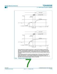
In order to fully charge the coupling capacitors at the inputs, the amplifier will remain
automatically in the Mute mode before switching to the Operating mode. A complete
overview of the start-up timing is given in Figure 5.
+
5 V
standby/
mute
R
MODE pin
R
C
mute/on
SGND
001aab172
Fig 4. Example of mode selection circuit.
9397 750 13356
© Koninklijke Philips Electronics N.V. 2004. All rights reserved.
Preliminary data sheet
Rev. 01 — 1 October 2004
6 of 34

 NXP [ NXP ]