TDA8920B
Philips Semiconductors
2 × 100 W class-D power amplifier
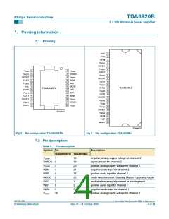
7. Pinning information
7.1 Pinning
1
2
OSC
IN1P
IN1M
3
V
4
DDA1
5
SGND1
V
6
SSA1
24
23
22
21
20
19
18
17
16
15
14
13
1
2
V
V
SSA2
SSD
7
PROT
V
SGND2
DDP2
V
8
DDP1
3
BOOT2
V
DDA2
9
BOOT1
OUT1
4
OUT2
IN2M
IN2P
MODE
OSC
10
11
12
13
14
15
16
17
18
19
20
21
22
23
5
V
SSP2
V
SSP1
6
n.c.
STABI
TDA8920BJ
TDA8920BTH
7
STABI
V
SSP2
8
V
SSP1
IN1P
IN1M
OUT2
9
OUT1
BOOT2
10
11
12
BOOT1
V
DDA1
V
DDP2
V
SGND1
DDP1
V
SSD
PROT
V
SSA1
V
SSA2
SGND2
001aab217
V
DDA2
IN2M
IN2P
MODE
001aab218
Fig 2. Pin configuration TDA8920BTH.
Fig 3. Pin configuration TDA8920BJ.
7.2 Pin description
Table 3:
Symbol Pin
TDA8920BTH TDA8920BJ
Pin description
Description
VSSA2
SGND2
VDDA2
IN2M
IN2P
1
2
18
19
20
21
22
23
1
negative analog supply voltage for channel 2
signal ground for channel 2
3
positive analog supply voltage for channel 2
negative audio input for channel 2
4
5
positive audio input for channel 2
MODE
OSC
6
mode selection input: Standby, Mute or Operating mode
oscillator frequency adjustment or tracking input
positive audio input for channel 1
7
IN1P
8
2
IN1M
VDDA1
9
3
negative audio input for channel 1
10
4
positive analog supply voltage for channel 1
9397 750 13356
© Koninklijke Philips Electronics N.V. 2004. All rights reserved.
Preliminary data sheet
Rev. 01 — 1 October 2004
4 of 34

 NXP [ NXP ]