Philips Semiconductors
Product specification
Dual common-mode rejection
differential line receiver
TDA8579
CHARACTERISTICS
V
CC = 8.5 V; Tamb = 25 °C; f = 1 kHz; measured in test circuit of Fig.3; unless otherwise specified.
SYMBOL PARAMETER CONDITIONS MIN. TYP.
VCC supply voltage 5.0 8.5
MAX.
18
UNIT
V
ICC
VO
tset
Gv
supply current
−
11
4.3
0.2
0
14
−
mA
V
DC output voltage
DC input voltage settling time
voltage gain
note 1
−
−
−
s
−0.5
70
−
+0.5
−
dB
dB
dB
Hz
kHz
kΩ
Ω
αcs
channel separation
channel unbalance
low frequency roll-off
high frequency roll-off
input impedance
Rs = 5 kΩ
80
−
∆Gv
0.5
−
fL
−1 dB; note 2
−1 dB
20
20
100
−
−
fH
−
−
Zi
240
−
−
Zo
output impedance
maximum input voltage
noise output voltage
10
−
Vi(max)
Vno
THD = 1%
−
2.0
3.7
−
V
Rs = 0 Ω; note 3
−
5.0
1.0
µV
V
VCM(rms)
common-mode input voltage
(RMS value)
−
CMRR
SVRR
THD
common-mode rejection ratio
supply voltage ripple rejection
total harmonic distortion
Rs = 5 kΩ
Rs = 0 Ω; note 4
note 5
66
−
70
80
65
60
0.02
−
−
dB
dB
dB
dB
%
−
55
−
−
note 6
−
Vi = 1 V;
−
−
Vi = 1 V;
−
0.1
%
f = 20 Hz to 20 kHz
THDmax
total harmonic distortion at
maximum output current
Vi = 1 V; RL = 150 Ω
−
−
1
%
Notes
1. The DC output voltage with respect to ground is approximately 0.5VCC
2. The frequency response is externally fixed by the input coupling capacitors.
3. The noise output voltage is measured in a bandwidth of 20 Hz to 20 kHz (unweighted).
.
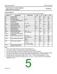
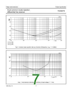
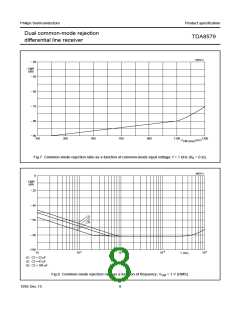
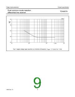
4. The common-mode rejection ratio is measured at the output with a voltage source 1 V (RMS) in accordance with the
test circuit (see Fig.3) while VINL and VINR are short-circuited. Frequencies between 100 Hz and 100 kHz.
5. The ripple rejection is measured at the output, with Rs = 2 kΩ, f = 1 kHz and a ripple amplitude of 2 V (p-p).
6. The ripple rejection is measured at the output, with Rs = 0 to 2 kΩ, f = 100 Hz to 20 kHz and a maximum ripple
amplitude of 2 V (p-p).
1995 Dec 15
5

 NXP [ NXP ]