Philips Semiconductors
Product specification
Dual common-mode rejection
differential line receiver
TDA8579
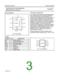
BLOCK DIAGRAM
FUNCTIONAL DESCRIPTION
The TDA8579 contains two identical differential amplifiers
with a voltage gain of 0 dB. The device is intended to
receive line input signals for audio applications. The
TDA8579 has a very high level of common-mode rejection
and thus eliminates ground noise. The common-mode
rejection remains constant up to high frequencies (the
amplifier gain is fixed at 0 dB). The inputs have a high input
impedance. The output stage is a class AB stage with a
low output impedance. For a large common-mode
rejection, also at low frequencies, an electrolytic capacitor
connected to the negative input is advised. Because the
input impedance is relatively high, this results in a large
settling time of the DC input voltage. Therefore a
quick-charge circuit is included to charge the input
capacitor within 0.2 seconds.
V
CC
8
1
INL
IN
7
OUTL
SVRR
OUTR
V
CC
2
3
4
TDA8579
6
INR
5
MBD230
GND
All input and output pins are protected against high
electrostatic discharge conditions (4000 V, 150 pF, 150 Ω).
Fig.1 Block diagram.
PINNING
SYMBOL PIN
DESCRIPTION
positive input left
INL+
IN−
1
2
3
4
5
6
7
8
V
INL
IN
1
2
3
4
8
7
6
5
CC
common negative input
positive input right
half supply voltage
ground
OUTL
OUTR
INR+
SVRR
GND
OUTR
OUTL
VCC
TDA8579
INR
SVRR
GND
output right
MBD231
output left
Fig.2 Pin configuration.
supply voltage
1995 Dec 15
3

 NXP [ NXP ]
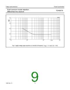