Philips Semiconductors
Product specification
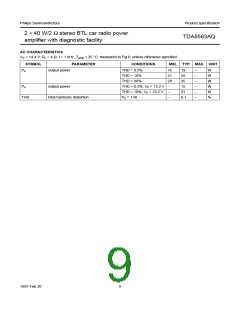
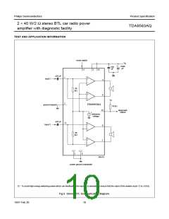
2 × 40 W/2 Ω stereo BTL car radio power
amplifier with diagnostic facility
TDA8563AQ
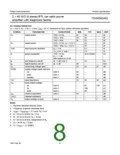
DC CHARACTERISTICS
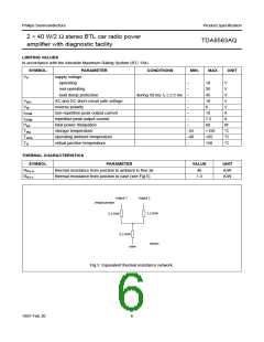
VP = 14.4 V; Tamb = 25 °C; measured in Fig.6; unless otherwise specified.
SYMBOL
Supply
PARAMETER
CONDITIONS
MIN. TYP. MAX. UNIT
VP
Iq
supply voltage
quiescent current
note 1
6.0
14.4
115
18
V
RL = ∞
−
180
mA
Operating condition
V11
I11
mode switch voltage level
8.5
−
−
VP
40
−
V
mode switch current
DC output voltage
V11 = 14.4 V
note 2
15
7.3
−
µA
V
VO
−
∆VO
DC output offset voltage
−
150
mV
Mute condition
V11
VO
mode switch voltage level
DC output voltage
3.3
−
−
6.4
−
V
note 2
7.3
−
V
∆VO
DC output offset voltage
−
150
mV
Standby condition
V11
Isb
mode switch voltage level
standby current
0
−
2
V
−
0.1
100
µA
Diagnostic output
V12
diagnostic output voltage
any short-circuit or clipping
−
−
0.6
V
Notes
1. The circuit is DC adjusted at VP = 6 to 18 V and AC operating at VP = 8.5 to 18 V.
2. At 18 V < VP < 30 V the DC output voltage ≤1⁄2VP.
1997 Feb 20
7

 NXP [ NXP ]