Philips Semiconductors
Product specification
2 × 40 W/2 Ω stereo BTL car radio power
amplifier with diagnostic facility
TDA8563AQ
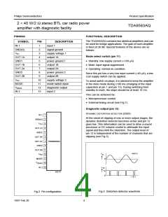
PINNING
SYMBOL
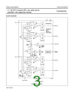
FUNCTIONAL DESCRIPTION
The TDA8563AQ contains two identical amplifiers and can
be used for bridge applications. The gain of each amplifier
is fixed at 26 dB. Special features of the device are as
follows.
PIN
DESCRIPTION
input 1
IN 1
1
2
GND(S)
VP1
signal ground
supply voltage 1
output 1A
3
Mode select switch (pin 11)
OUT 1A
GND1
OUT 1B
OUT 2A
GND2
OUT 2B
VP2
4
• Standby: low supply current (<100 µA)
• Mute: input signal suppressed
5
power ground 1
output 1B
6
7
output 2A
• Operating: normal on condition.
8
power ground 2
output 2B
Since this pin has a very low input current (<40 µA), a low
cost supply switch can be applied.
9
10
11
12
13
supply voltage 2
mode switch input
diagnostic output
input 2
To avoid switch-on plops, it is advised to keep the amplifier
in the mute mode during ≥100 ms (charging of the input
capacitors at pin 1 and pin 13). During switching from
standby to mute, the slope should be at least 18 V/s.
MODE
VDIAG
IN 2
This can be achieved by:
• Microprocessor control
• External timing circuit (see Fig.7).
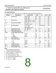
Diagnostic output (pin 12)
handbook, halfpage
DYNAMIC DISTORTION DETECTOR (DDD)
IN 1
1
2
At the onset of clipping of one or more output stages, the
dynamic distortion detector becomes active and pin 12
goes low. This information can be used to drive a sound
processor or DC volume control to attenuate the input
signal and thus limit the distortion. The output level of
pin 12 is independent of the number of channels that are
clipping (see Fig.3).
GND(S)
V
3
P1
OUT 1A
GND1
4
5
OUT 1B
OUT 2A
GND2
6
7
TDA8563AQ
8
OUT 2B
9
MGA721
V
handbook, halfpage
V
10
11
12
P2
O
MODE
0
V
DIAG
IN 2 13
V
12
V
P
MGL075
0
t
Fig.3 Distortion detector waveform.
Fig.2 Pin configuration.
1997 Feb 20
4

 NXP [ NXP ]