Philips Semiconductors
Preliminary specification
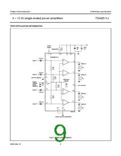
4 × 13 W single-ended power amplifiers
TDA8511J
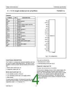
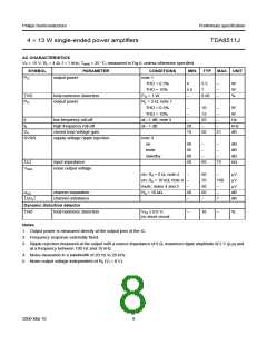
PINNING
SYMBOL
IN1
PIN
DESCRIPTION
1
2
3
4
5
6
7
8
9
input 1
handbook, halfpage
IN1
SGND
IN2
1
2
3
4
5
6
7
8
9
SGND
IN2
signal ground
input 2
RR
supply voltage ripple rejection
supply voltage
output 1
VP1
RR
OUT1
GND1
OUT2
n.c.
V
P1
power ground 1
output 2
OUT1
GND1
OUT2
n.c.
not connected
OUT3
GND2
OUT4
VP2
10 output 3
TDA8511J
11 power ground 2
12 output 4
OUT3 10
GND2 11
OUT4 12
13 supply voltage
14 mode select switch input
15 input 3
MODE
IN3
V
13
P2
VDIAG
IN4
16 diagnostic output
17 input 4
MODE 14
IN3 15
V
16
DIAG
IN4 17
MGL498
Fig.2 Pin configuration.
FUNCTIONAL DESCRIPTION
This can be achieved by:
• Microprocessor control
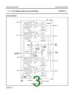
The TDA8511J contains four identical amplifiers and can
be used for single-ended applications. The gain of each
amplifier is fixed at 20 dB. Special features of the device
are:
• External timing circuit (see Fig.7).
Diagnostic output (pin 16)
• Mode select switch (pin 14)
• Diagnostic output (pin 16).
DYNAMIC DISTORTION DETECTOR (DDD)
At the onset of clipping of one or more output stages, the
dynamic distortion detector becomes active and pin 16
goes LOW. This information can be used to drive a sound
processor or DC volume control to attenuate the input
signal and thus limit the distortion. The output level of
pin 16 is independent of the number of channels that are
clipping (see Fig.3).
Mode select switch (pin 14)
• Low standby current (<100 µA)
• Low switching current (low cost supply switch)
• Mute facility.
To avoid switch-on plops, it is advised to keep the amplifier
in the mute mode during ≥100 ms (charging of the input
capacitors at pin 1, 3, 15 and pin 17).
2000 Mar 10
4

 NXP [ NXP ]