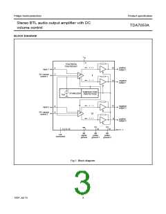
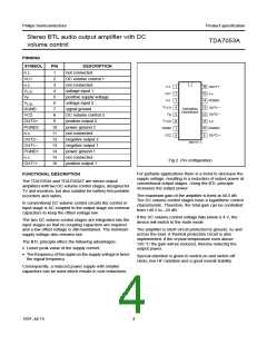
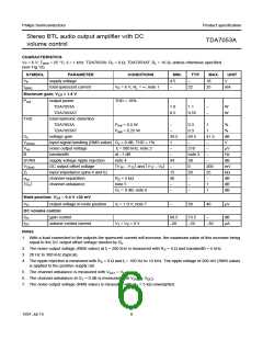
Philips Semiconductors
Product specification
Stereo BTL audio output amplifier with DC
volume control
TDA7053A
CHARACTERISTICS
VP = 6 V; Tamb = 25 °C; fi = 1 kHz; TDA7053A: RL = 8 Ω; TDA7053AT: RL = 16 Ω; unless otherwise specified
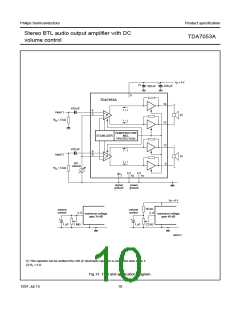
(see Fig.13).
SYMBOL
VP
Iq(tot)
Maximum gain; V2,8 ≥ 1.4 V
PARAMETER
supply voltage
total quiescent current
CONDITIONS
MIN.
4.5
TYP.
MAX.
18
UNIT
−
V
VP = 6 V; RL = ∞; note 1
−
22
25
mA
Pout
output power
TDA7053A
THD = 10%
1.0
0.5
1.1
−
−
W
W
TDA7053AT
0.55
THD
total harmonic distortion
TDA7053A
P
out = 0.5 W
−
0.3
0.3
40.5
−
1
%
TDA7053AT
Pout = 0.25 W
−
1
%
Gv
voltage gain
39.5
1
41.5
−
dB
V
VI(rms)
Vno
B
input signal handling (RMS value) Gv = 0 dB; THD < 1%
noise output voltage
bandwidth
fi = 500 kHz; note 2
at −1 dB
−
210
note 3
38
0
−
µV
Hz
dB
mV
kΩ
dB
dB
dB
−
−
SVRR
VO(os)
Zi
supply voltage ripple rejection
DC output offset voltage
input impedance (pins 4 and 6)
channel separation
note 4
34
−
−
V16 − V13 and V12 − V9
200
25
−
15
40
−
20
−
αcs
RS = 5 kΩ
Gv
channel unbalance
note 5
−
1
G1 = 0 dB; note 6
−
−
1
Mute position; V2,8 = 0.4 V ±30 mV
VO
output voltage in mute position
Vi = 1.0 V; note 7
V2 = V8 = 0 V
−
30
40
µV
DC volume control
GC
IDC
gain control
volume control current
68.5
73.5
−
dB
−20
−25
−30
µA
Notes
1. With a load connected to the outputs the quiescent current will increase, the maximum value of this increase being
equal to the DC output offset voltage divided by RL.
2. The noise output voltage (RMS value) at fi = 500 kHz is measured with RS = 0 Ω and bandwidth = 5 kHz.
3. 20 Hz to 300 kHz (typical).
4. The ripple rejection is measured with RS = 0 Ω and fi = 100 Hz to 10 kHz. The ripple voltage of 200 mV (RMS value)
is applied to the positive supply rail.
5. The channel unbalance is measured with VDC1 = VDC2
6. The channel unbalance at G1 = 0 dB is measured with VDC1 = VDC2
7. The noise output voltage (RMS value) is measured with RS = 5 kΩ unweighted.
.
.
1997 Jul 15
6

 NXP [ NXP ]