Philips Semiconductors
Product specification
Triple video output amplifier
TDA6108JF
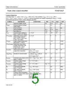
SYMBOL
∆tPco
PARAMETER
CONDITIONS
MIN.
−10
TYP.
MAX.
+10
UNIT
ns
difference in cathode output
V
o(c) = 100 V (p-p)
0
propagation time 50% input to square wave; f < 1 MHz;
50% output (pins 7 and 8,
7 and 9 and 8 and 9)
tr = tf = 40 ns
(pins 1, 2 and 3)
to(r)
to(f)
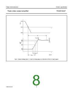
tst
cathode output rise time
10% output to 90% output
(pins 7, 8 and 9)
Vo(c) = 50 to 150 V square
wave; f < 1 MHz; tf = 40 ns
(pins 1, 2 and 3); see Fig.6
35
35
−
50
50
−
65
ns
ns
ns
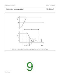
cathode output fall time
90% output to 10% output
(pins 7, 8 and 9)
Vo(c) = 150 to 50 V square
wave; f < 1 MHz; tr = 40 ns
(pins 1, 2 and 3); see Fig.7
65
settling time 50% input to
99% < output < 101%
(pins 7, 8 and 9)
Vo(c) = 100 V (p-p)
square wave; f < 1 MHz;
tr = tf = 40 ns
350
(pins 1, 2 and 3);
see Figs 6 and 7
SR
Ov
slew rate between
50 V to (VDD − 50 V)
(pins 7, 8 and 9)
Vi = 4 V (p-p) square wave;
f < 1 MHz; tr = tf = 40 ns
(pins 1, 2 and 3)
−
−
1850
10
−
−
V/µs
cathode output voltage
overshoot (pins 7, 8 and 9)
Vo(c) = 100 V (p-p)
square wave; f < 1 MHz;
tr = tf = 40 ns
%
(pins 1, 2 and 3);
see Figs 6 and 7
PSRR
power supply rejection ratio
f < 50 kHz; note 2
−
−
65
50
−
−
dB
dB
αct(DC)
DC crosstalk between
channels
Notes
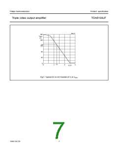
1. See also Fig.5 for the typical DC-to-DC transfer of Vi to Vo(c)
.
2. The ratio of the change in supply voltage to the change in input voltage when there is no change in output voltage.
1999 Oct 29
6

 NXP [ NXP ]