Philips Semiconductors
Product specification
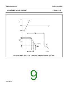
Triple video output amplifier
TDA6108JF
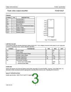
PINNING
SYMBOL
PIN
DESCRIPTION
inverting input 1
Vi(1)
1
2
3
4
5
6
7
8
9
handbook, halfpage
V
V
V
1
2
3
4
5
6
7
8
9
i(1)
i(2)
i(3)
Vi(2)
inverting input 2
Vi(3)
inverting input 3
GND
Iom
ground (fin)
black current measurement output
supply voltage
GND
VDD
I
om
TDA6108JF
Voc(3)
Voc(2)
Voc(1)
cathode output 3
cathode output 2
cathode output 1
V
DD
V
V
V
oc(3)
oc(2)
oc(1)
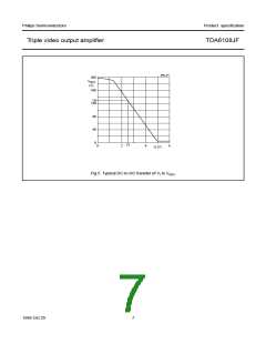
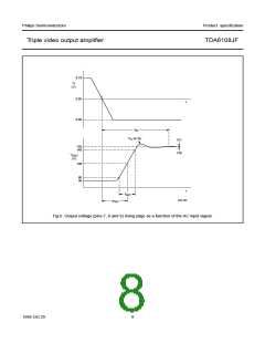
MGL319
Fig.2 Pin configuration.
LIMITING VALUES
In accordance with the Absolute Maximum Rating System (IEC 134); voltages measured with respect to pin 4 (ground);
currents as specified in Fig.1; unless otherwise specified.
SYMBOL
PARAMETER
MIN.
MAX.
250
UNIT
VDD
Vi
supply voltage
input voltage
0
0
0
0
V
12
V
Vom
Voc
Tstg
Tj
measurement output voltage
cathode output voltage
storage temperature
6
V
VDD
+150
+150
V
−55
−20
°C
°C
junction temperature
Ves
electrostatic handling
human body model (HBM)
machine model (MM)
−
−
2000
300
V
V
HANDLING
Inputs and outputs are protected against electrostatic discharge in normal handling. However, to be totally safe, it is
desirable to take normal precautions appropriate to handling MOS devices (see “Handling MOS Devices”).
QUALITY SPECIFICATION
Quality specification “SNW-FQ-611 part D” is applicable.
1999 Oct 29
3

 NXP [ NXP ]