Philips Semiconductors
Product specification
Triple video output amplifier
TDA6107Q
PINNING
SYMBOL
PIN
DESCRIPTION
inverting input 1
Vi(1)
1
2
3
4
5
6
7
8
9
handbook, halfpage
Vi(2)
inverting input 2
V
V
V
1
2
3
4
5
6
7
8
9
i(1)
i(2)
i(3)
Vi(3)
inverting input 3
GND
Iom
ground (fin)
black-current measurement output
supply voltage
GND
VDD
I
om
Voc(3)
Voc(2)
Voc(1)
cathode output 3
cathode output 2
cathode output 1
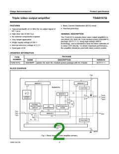
TDA6107Q
V
DD
V
V
V
oc(3)
oc(2)
oc(1)
MGK277
Fig.2 Pin configuration.
LIMITING VALUES
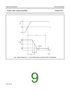
In accordance with the Absolute Maximum Rating System (IEC 134); voltages measured with respect to pin 4 (ground);
currents as specified in Fig.1; unless otherwise specified.
SYMBOL
PARAMETER
MIN.
MAX.
250
UNIT
VDD
Vi
supply voltage
0
0
0
0
V
input voltage at pins 1 to 3
12
V
Vo(m)
Vo(c)
Tstg
Tj
measurement output voltage
cathode output voltage
storage temperature
6
V
VDD
+150
+150
V
−55
−20
°C
°C
junction temperature
Ves
electrostatic handling
Human Body Model (HBM)
Machine Model (MM)
−
−
2000
300
V
V
HANDLING
Inputs and outputs are protected against electrostatic discharge in normal handling. However, to be totally safe, it is
desirable to take normal precautions appropriate to handling MOS devices (see “Handling MOS Devices”).
QUALITY SPECIFICATION
Quality specification “SNW-FQ-611 part D” is applicable and can be found in the “Quality reference Handbook”.
The handbook can be ordered using the code 9397 750 00192.
1999 Oct 26
3

 NXP [ NXP ]