Philips Semiconductors
Product specification
24 W BTL or 2 x 12 W stereo
car radio power amplifier
TDA1515BQ
<
50 mV
2 mV
D.C. output offset voltage between the outputs
|∆V
|
|
5-9
typ.
Loudspeaker protection (all conditions)
maximum d.c. voltage (across the load)
|∆V
<
1 V
5-9
Power bandwidth; −1 dB; d = 0,5%
B
30 Hz to 40 kHz
tot
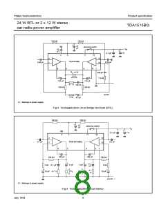
Stereo application; see Fig.4
Output power at d = 10%; with bootstrap (note 6)
tot
>
6 W
7 W
V = 14,4 V; R = 4 Ω
P
P
P
L
o
typ.
>
10 W
12 W
6 W
V = 14,4 V; R = 2 Ω
P
L
o
typ.
typ.
typ.
V = 13,2 V; R = 4 Ω
P
P
P
L
o
V = 13,2 V; R = 2 Ω
10 W
P
L
o
Output power at d = 0,5%; with bootstrap (note 6)
tot
V = 14,4 V; R = 4 Ω
P
P
P
P
typ.
typ.
typ.
typ.
5,5 W
9 W
P
L
o
o
o
o
V = 14,4 V; R = 2 Ω
P
L
V = 13,2 V; R = 4 Ω
4,5 W
7,5 W
P
L
V = 13,2 V; R = 2 Ω
P
L
Output power at d = 10%; without bootstrap
tot
V = 14,4 V; R = 4 Ω (notes 6, 8 and 9)
P
B
typ.
6 W
40 Hz to min. 20 kHz
50 dB
P
L
o
Frequency response at −3 dB (note 3)
Supply voltage ripple rejection (note 5)
RR
typ.
>
40 dB
Channel separation; R = 10 kΩ; f = 1 kHz
α
S
typ.
typ.
50 dB
Closed loop voltage gain (note 7)
G
40 dB
c
Noise output voltage (r.m.s. value) at f = 20 Hz to 20 kHz
R = 0 Ω
V
V
V
typ.
typ.
typ.
0,15 mV
0,25 mV
0,2 mV
S
n(rms)
n(rms)
n
R = 10 kΩ
S
R = 10 kΩ; according to IEC 179 curve A
S
Notes
1. The internal circuit impedance at pin 11 is > 5 kΩ if V > V .
11
10
2. Closed loop voltage gain can be chosen between 32 and 56 dB (BTL), and is determined by external components.
For further gain reduction see Application Report.
3. Frequency response externally fixed.
4. The input impedance in the test circuit (Fig.3) is typ. 100 kΩ.
5. Supply voltage ripple rejection measured with a source impedance of 0 Ω (maximum ripple amplitude: 2 V).
6. Output power is measured directly at the output pins of the IC.
7. Closed loop voltage gain can be chosen between 26 and 50 dB (stereo), and is determined by external components.
8. A resistor of 56 kΩ between pins 3 and 7 to reach symmetrical clipping.
9. Without bootstrap the 100 µF capacitor between pins 5 and 6 (8 and 9) can be omitted. Pins 6, 8 and 10 have to be
interconnected.
July 1994
7

 NXP [ NXP ]