Philips Semiconductors
Product specification
24 W BTL or 2 x 12 W stereo
car radio power amplifier
TDA1515BQ
D.C. CHARACTERISTICS
Supply voltage range (pin 10)
Repetitive peak output current
Total quiescent current
V
6 to 18 V
4 A
P
I
I
<
ORM
tot
typ.
<
75 mA
1,8 V
Switching level 11:
OFF
ON
V
V
11
11
>
3 V
Impedance between pins 10 and 6; 10 and 8 (stand-by position V < 1,8 V)
|Z
|
>
100 kΩ
1 µA
11
OFF
typ.
<
Stand-by current at V = 0 to 0,8 V
I
11
sb
100 µA
10 µA
100 µA
typ.
<
Switch-on current (pin 11) at V ≤ V (note 1)
I
11
10
so
A.C. CHARACTERISTICS
= 25 °C; V = 14,4 V; f = 1 kHz; unless otherwise specified
T
amb
P
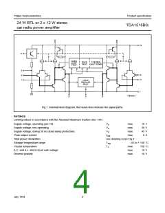
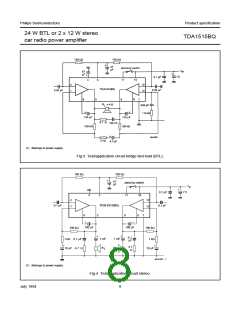
Bridge tied load application (BTL); see Fig.3
Output power at R = 4 Ω (with bootstrap)
L
>
15,5 W
18 W
V = 14,4 V; d = 0,5%
P
P
P
tot
o
typ.
>
20 W
V = 14,4 V; d = 10%
P
tot
o
typ.
typ.
typ.
typ.
typ.
24 W
V = 13,2 V; d = 0,5%
P
P
15 W
P
tot
o
V = 13,2 V; d = 10%
20 W
P
tot
o
Open loop voltage gain
G
G
75 dB
o
Closed loop voltage gain (note 2)
Output power without bootstrap (note 9)
40 (± 0,5) dB
c
V = 14,4 V; d = 10%
P
P
P
P
B
typ.
typ.
typ.
typ.
15 W
12 W
12 W
9 W
P
tot
o
V = 14,4 V; d = 0,5%
P
tot
o
o
o
V = 13,2 V; d = 10%
P
tot
V = 13,2 V; d = 0,5%
P
tot
Frequency response at −3 dB (note 3)
Input impedance (note 4)
20 Hz to min. 20 kHz
|Z |
>
1 MΩ
i
Noise input voltage (r.m.s. value) at f = 20 Hz to 20 kHz
R = 0 Ω
V
V
V
typ.
typ.
<
0,2 mV
0,35 mV
0,8 mV
S
n(rms)
n(rms)
n
R = 10 kΩ
S
R = 10 kΩ; according to IEC 179 curve A
typ.
0,25 mV
S
Supply voltage ripple rejection (note 5)
>
42 dB
50 dB
f = 100 Hz
RR
typ.
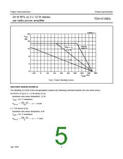
July 1994
6

 NXP [ NXP ]