Philips Semiconductors
Product specification
CMOS single-chip 8-bit microcontrollers
80C31/80C51/87C51
EPROM CHARACTERISTICS
The 87C51 is programmed by using a modified Quick-Pulse
Programming algorithm. It differs from older methods in the value
Program Verification
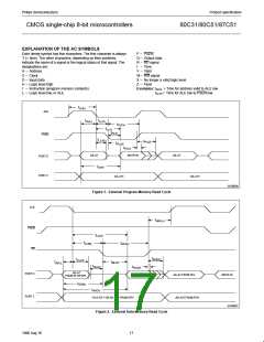
If security bit 2 has not been programmed, the on-chip program
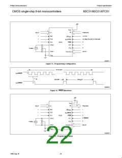
memory can be read out for program verification. The address of the
program memory locations to be read is applied to ports 1 and 2 as
shown in Figure 15. The other pins are held at the ‘Verify Code Data’
levels indicated in Table 3. The contents of the address location will
be emitted on port 0. External pull-ups are required on port 0 for this
operation.
used for V (programming supply voltage) and in the width and
PP
number of the ALE/PROG pulses.
The 87C51 contains two signature bytes that can be read and used
by an EPROM programming system to identify the device. The
signature bytes identify the device as an 87C51 manufactured by
Philips Corporation.
If the encryption table has been programmed, the data presented at
port 0 will be the exclusive NOR of the program byte with one of the
encryption bytes. The user will have to know the encryption table
contents in order to correctly decode the verification data. The
encryption table itself cannot be read out.
Table 3 shows the logic levels for reading the signature bytes, and
for programming the program memory, the encryption table, and the
security bits. The circuit configuration and waveforms for quick-pulse
programming are shown in Figures 13 and 14. Figure 15 shows the
circuit configuration for normal program memory verification.
Reading the Signature Bytes
The signature bytes are read by the same procedure as a normal
verification of locations 030H and 031H, except that P3.6 and P3.7
need to be pulled to a logic low. The values are:
(030H) = 15H indicates manufactured by Philips
(031H) = 92H indicates 87C51
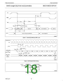
Quick-Pulse Programming
The setup for microcontroller quick-pulse programming is shown in
Figure 13. Note that the 87C51 is running with a 4 to 6MHz
oscillator. The reason the oscillator needs to be running is that the
device is executing internal address and program data transfers.
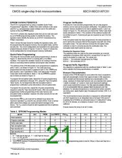
Program/Verify Algorithms
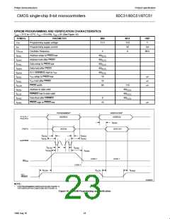
Any algorithm in agreement with the conditions listed in Table 3, and
which satisfies the timing specifications, is suitable.
The address of the EPROM location to be programmed is applied to
ports 1 and 2, as shown in Figure 13. The code byte to be
programmed into that location is applied to port 0. RST, PSEN and
pins of ports 2 and 3 specified in Table 3 are held at the ‘Program
Code Data’ levels indicated in Table 3. The ALE/PROG is pulsed
low 25 times as shown in Figure 14.
Erasure Characteristics
Erasure of the EPROM begins to occur when the chip is exposed to
light with wavelengths shorter than approximately 4,000 angstroms.
Since sunlight and fluorescent lighting have wavelengths in this
range, exposure to these light sources over an extended time (about
1 week in sunlight, or 3 years in room level fluorescent lighting)
could cause inadvertent erasure. For this and secondary effects,
it is recommended that an opaque label be placed over the
window. For elevated temperature or environments where solvents
are being used, apply Kapton tape Fluorglas part number 2345–5, or
equivalent.
To program the encryption table, repeat the 25 pulse programming
sequence for addresses 0 through 1FH, using the ‘Pgm Encryption
Table’ levels. Do not forget that after the encryption table is
programmed, verification cycles will produce only encrypted data.
To program the security bits, repeat the 25 pulse programming
sequence using the ‘Pgm Security Bit’ levels. After one security bit is
programmed, further programming of the code memory and
encryption table is disabled. However, the other security bit can still
be programmed.
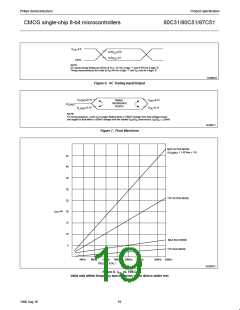
The recommended erasure procedure is exposure to ultraviolet light
(at 2537 angstroms) to an integrated dose of at least 15W-sec/cm .
Exposing the EPROM to an ultraviolet lamp of 12,000µW/cm rating
for 20 to 39 minutes, at a distance of about 1 inch, should be
sufficient.
2
Note that the EA/V pin must not be allowed to go above the
PP
2
maximum specified V level for any amount of time. Even a narrow
PP
glitch above that voltage can cause permanent damage to the
device. The V source should be well regulated and free of glitches
PP
and overshoot.
Erasure leaves the array in an all 1s state.
Table 3. EPROM Programming Modes
MODE
Read signature
RST
PSEN
ALE/PROG
EA/V
P2.7
P2.6
P3.7
P3.6
PP
1
1
1
1
1
1
0
0
0
0
0
0
1
1
0
1
0
1
1
1
0
0
0
0
1
1
0
1
1
1
1
0
0
1
1
0
1
0
Program code data
Verify code data
Pgm encryption table
Pgm security bit 1
0*
1
V
PP
1
0*
0*
0*
V
PP
PP
PP
V
V
Pgm security bit 2
NOTES:
1. ‘0’ = Valid low for that pin, ‘1’ = valid high for that pin.
2. V = 12.75V +0.25V.
PP
3. V = 5V±10% during programming and verification.
CC
4. *ALE/PROG receives 25 programming pulses while V is held at 12.75V. Each programming pulse is low for 100µs (±10µs) and high for a
PP
minimum of 10µs.
Trademark phrase of Intel Corporation.
21
1996 Aug 16

 NXP [ NXP ]