Philips Semiconductors
Product specification
Clock/calendar with 240 × 8-bit RAM
PCF8583
5
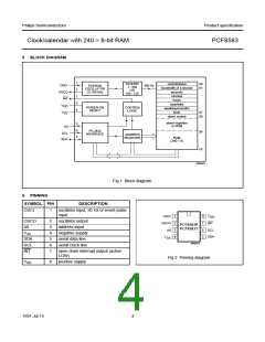
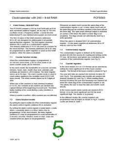
BLOCK DIAGRAM
handbook, full pagewidth
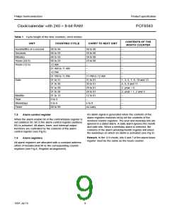
1
2
7
8
4
DIVIDER
1 : 256
OR
control/status
hundredth of a second
seconds
00
01
OSCI
OSCO
INT
100 Hz
PCF8583
OSCILLATOR
32.768 kHz
100 : 128
minutes
hours
year/date
V
DD
POWER-ON
RESET
CONTROL
LOGIC
weekdays/months
timer
V
07
08
SS
alarm control
alarm registers
or RAM
3
A0
2
6
5
I C-BUS
0F
FF
SCL
SDA
INTERFACE
ADDRESS
REGISTER
RAM
(240 × 8)
MRB001
Fig.1 Block diagram.
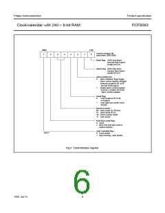
6
PINNING
SYMBOL PIN
DESCRIPTION
OSCI
1
oscillator input, 50 Hz or event-pulse
input
handbook, halfpage
V
1
2
3
4
8
7
OSCI
OSCO
A0
DD
OSCO
A0
2
3
4
5
6
7
oscillator output
address input
INT
PCF8583P
PCF8583T
6
5
SCL
SDA
VSS
negative supply
serial data line
serial clock line
V
SS
SDA
SCL
INT
MRB014
open drain interrupt output (active
LOW)
Fig.2 Pinning diagram.
VDD
8
positive supply
1997 Jul 15
4

 NXP [ NXP ]