Philips Semiconductors
Product specification
Clock/calendar with 240 × 8-bit RAM
PCF8583
1
FEATURES
2
GENERAL DESCRIPTION
• I2C-bus interface operating supply voltage: 2.5 V to 6 V
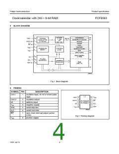
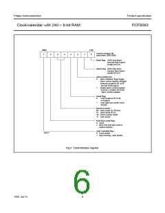
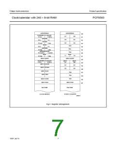
The PCF8583 is a clock/calendar circuit based on a
2048-bit static CMOS RAM organized as 256 words by
8 bits. Addresses and data are transferred serially via the
two-line bidirectional I2C-bus. The built-in word address
register is incremented automatically after each written or
read data byte. Address pin A0 is used for programming
the hardware address, allowing the connection of two
devices to the bus without additional hardware.
• Clock operating supply voltage (0 to +70 °C):
1.0 V to 6.0 V
• 240 × 8-bit low-voltage RAM
• Data retention voltage: 1.0 V to 6 V
• Operating current (at fSCL = 0 Hz): max. 50 µA
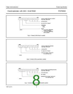
• Clock function with four year calendar
• Universal timer with alarm and overflow indication
• 24 or 12 hour format
The built-in 32.768 kHz oscillator circuit and the first
8 bytes of the RAM are used for the clock/calendar and
counter functions. The next 8 bytes may be programmed
as alarm registers or used as free RAM space.
• 32.768 kHz or 50 Hz time base
• Serial input/output bus (I2C)
The remaining 240 bytes are free RAM locations.
• Automatic word address incrementing
• Programmable alarm, timer and interrupt function
• Slave address:
– READ: A1 or A3
– WRITE: A0 or A2.
3
QUICK REFERENCE DATA
SYMBOL
VDD
PARAMETER
CONDITION
I2C-bus active
I2C-bus inactive
MIN.
2.5
TYP.
MAX.
6.0
UNIT
supply voltage operating mode
−
−
−
V
1.0
−
6.0
V
IDD
supply current operating mode
supply current clock mode
fSCL = 100 kHz
200
50
µA
µA
µA
°C
°C
IDDO
fSCL = 0 Hz; VDD = 5 V
−
10
2
fSCL = 0 Hz; VDD = 1 V
−
10
Tamb
Tstg
operating ambient temperature range
storage temperature range
−40
−65
−
+85
+150
−
4
ORDERING INFORMATION
PACKAGE
TYPE
NUMBER
NAME
DESCRIPTION
VERSION
PCF8583P
PCF8583T
DIP8
SO8
plastic dual in-line package; 8 leads (300 mil)
plastic small outline package; 8 leads; body width 7.5 mm
SOT97-1
SOT176-1
1997 Jul 15
3

 NXP [ NXP ]