Philips Semiconductors
Product specification
Clock/calendar with 240 × 8-bit RAM
PCF8583
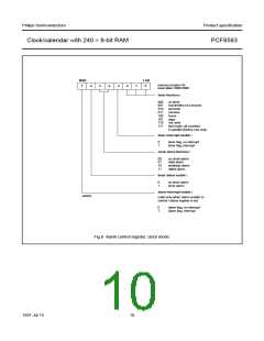
MSB
7
LSB
0
handbook, full pagewidth
memory location 08
reset state: 0000 0000
6
5
4
3
2
1
timer function :
000
001
010
011
100
101
110
111
no timer
units
100
10 000
1 000 000
not allowed
not allowed
test mode, all counters
in parallel
timer interrupt enable :
0
1
timer flag, no interrupt
timer flag, interrupt
clock alarm function :
00
01
10
11
no event alarm
event alarm
not allowed
not allowed
timer alarm enable :
0
1
no timer alarm
timer alarm
alarm interrupt enable :
MRB007
0
1
alarm flag, no interrupt
alarm flag, interrupt
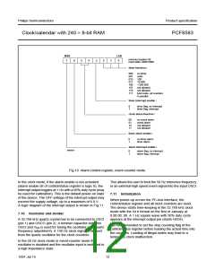
Fig.10 Alarm control register, event-counter mode.
In the clock mode, if the alarm enable is not activated
(alarm enable bit of control/status register is logic 0), the
interrupt output toggles at 1 Hz with a 50% duty cycle (may
be used for calibration). This is the default power-on state
of the device. The OFF voltage of the interrupt output may
exceed the supply voltage, up to a maximum of 6.0 V.
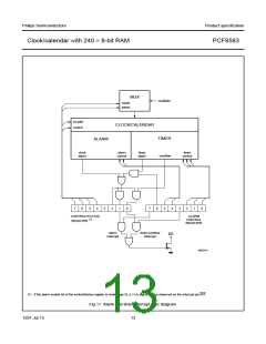
A logic diagram of the interrupt output is shown in Fig.11.
This allows the user to feed the 50 Hz reference frequency
or an external high speed event signal into the input OSCI.
7.11 Initialization
When power-up occurs the I2C-bus interface, the
control/status register and all clock counters are reset.
The device starts time-keeping in the 32.768 kHz clock
mode with the 24 h format on the first of January at
0.00.00: 00. A 1 Hz square wave with 50% duty cycle
appears at the interrupt output pin (starts HIGH).
7.10 Oscillator and divider
A 32.768 kHz quartz crystal has to be connected to OSCI
(pin 1) and OSCO (pin 2). A trimmer capacitor between
OSCI and VDD is used for tuning the oscillator (see quartz
frequency adjustment). A 100 Hz clock signal is derived
from the quartz oscillator for the clock counters.
It is recommended to set the stop counting flag of the
control/status register before loading the actual time into
the counters. Loading of illegal states may lead to a
temporary clock malfunction.
In the 50 Hz clock mode or event-counter mode the
oscillator is disabled and the oscillator input is switched to
a high impedance state.
1997 Jul 15
12

 NXP [ NXP ]