Philips Semiconductors
Product specification
Clock/calendar with 240 × 8-bit RAM
PCF8583
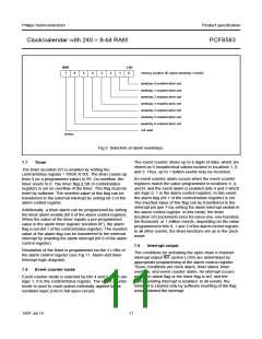
MSB
7
LSB
0
handbook, full pagewidth
6
5
4
3
2
1
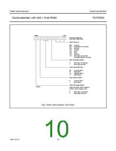
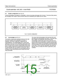
memory location 0E (alarm weekday / month)
weekday 0 enabled when set
weekday 1 enabled when set
weekday 2 enabled when set
weekday 3 enabled when set
weekday 4 enabled when set
weekday 5 enabled when set
weekday 6 enabled when set
not used
MRB006
Fig.9 Selection of alarm weekdays.
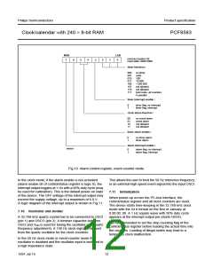
The event counter stores up to 6 digits of data, which are
stored as 6 hexadecimal values located in locations 1, 2,
and 3. Thus, up to 1 million events may be recorded.
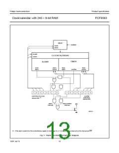
7.7
Timer
The timer (location 07) is enabled by setting the
control/status register = XX0X X1XX. The timer counts up
from 0 (or a programmed value) to 99. On overflow, the
timer resets to 0. The timer flag (LSB of control/status
register) is set on overflow of the timer. This flag must be
reset by software. The inverted value of this flag can be
transferred to the external interrupt by setting bit 3 of the
alarm control register.
An event counter alarm occurs when the event counter
registers match the value programmed in locations 9, A,
and B, and the event alarm is enabled (bits 4 and 5 which
are logic 0, 1 in the alarm control register). In this event,
the alarm flag (bit 1 of the control/status register) is set.
The inverted value of this flag can be transferred to the
interrupt pin (pin 7) by setting the alarm interrupt enable in
the alarm control register. In this mode, the timer
(location 07) increments once for every one, one-hundred,
ten thousand, or 1 million events, depending on the value
programmed in bits 0, 1 and 2 of the alarm control register.
In all other events, the timer functions are as in the clock
mode.
Additionally, a timer alarm can be programmed by setting
the timer alarm enable (bit 6 of the alarm control register).
When the value of the timer equals a pre-programmed
value in the alarm timer register (location 0F), the alarm
flag is set (bit 1 of the control/status register). The inverted
value of the alarm flag can be transferred to the external
interrupt by enabling the alarm interrupt (bit 6 of the alarm
control register).
7.9
Interrupt output
Resolution of the timer is programmed via the 3 LSBs of
the alarm control register (see Fig.11, Alarm and timer
Interrupt logic diagram).
The conditions for activating the open-drain n-channel
interrupt output INT (active LOW) are determined by
appropriate programming of the alarm control register.
These conditions are clock alarm, timer alarm, timer
overflow, and event counter alarm. An interrupt occurs
when the alarm flag or the timer flag is set, and the
corresponding interrupt is enabled. In all events, the
interrupt is cleared only by software resetting of the flag
which initiated the interrupt.
7.8
Event counter mode
Event counter mode is selected by bits 4 and 5 which are
logic 1, 0 in the control/status register. The event counter
mode is used to count pulses externally applied to the
oscillator input (OSCO left open-circuit).
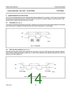
1997 Jul 15
11

 NXP [ NXP ]