PCF8583
NXP Semiconductors
Clock and calendar with 240 x 8-bit RAM
10.2 Dynamic characteristics
Table 8.
Dynamic characteristics
VDD = 2.5 V to 6.0 V; VSS = 0 V; Tamb = −40 °C to +85 °C unless otherwise specified.
Symbol
Oscillator
COSCO
Parameter
Conditions
Min
Typ
Max
Unit
capacitance on pin OSCO
-
-
40
-
-
pF
Δfosc/fosc
relative oscillator frequency
variation
for ΔVDD = 100 mV; Tamb = 25 °C;
0.2
ppm
VDD = 1.5 V
[1]
fclk(ext)
external clock frequency
on pin OSCI
-
-
1
MHz
Quartz crystal parameters (f = 32.768 kHz)
RS
series resistance
-
-
40
-
kΩ
pF
pF
CL
parallel load capacitance
-
10
-
Ctrim
trimmer capacitance
5
25
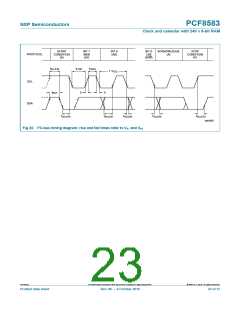
I2C-bus timing (see Figure 21)[2]
fSCL
tSP
SCL clock frequency
-
-
-
-
100
100
kHz
ns
pulse width of spikes that
must be suppressed by the
input filter
tBUF
bus free time between a
STOP and START condition
4.7
4.7
4.0
-
-
-
-
-
-
μs
μs
μs
tSU;STA
tHD;STA
set-up time for a repeated
START condition
hold time (repeated) START
condition
tLOW
tHIGH
tr
LOW period of the SCL clock
HIGH period of the SCL clock
4.7
4.0
-
-
-
-
-
μs
μs
μs
-
rise time of both SDA and
SCL signals
1.0
tf
fall time of both SDA and SCL
signals
-
-
0.3
μs
tSU;DAT
tHD;DAT
tVD;DAT
tSU;STO
data set-up time
data hold time
data valid time
250
0
-
-
-
-
-
ns
ns
μs
μs
-
-
3.4
-
set-up time for STOP
condition
4.0
[1] Event counter mode only.
[2] All timing values are valid within the operating supply voltage, ambient temperature range, reference to VIL and VIH and with an input
voltage swing of VSS to VDD
.
PCF8583
All information provided in this document is subject to legal disclaimers.
© NXP B.V. 2010. All rights reserved.
Product data sheet
Rev. 06 — 6 October 2010
22 of 37

 NXP [ NXP ]