Philips Semiconductors
Product specification
Remote 16-bit I/O expander for I2C-bus
PCF8575
7.3
Reading from a port (input mode)
7.5
Interrupt
All ports programmed as input should be set to logic 1.
To read, the master (microcontroller) first addresses the
slave device after it receives the interrupt. By setting the
last bit of the byte containing the slave address to logic 1
the read mode is entered. The data bytes that follow on the
SDA are the values on the ports.
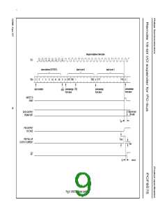
The PCF8575 provides an open-drain interrupt (INT)
which can be fed to a corresponding input of the
microcontroller (see Figs 9, 10 and 12). This gives these
chips a kind of a master function which can initiate an
action elsewhere in the system.
An interrupt is generated by any rising or falling edge of the
port inputs. After time tiv the signal INT is valid.
If the data on the input port changes faster than the master
can read, this data may be lost.
The interrupt disappears when data on the port is changed
to the original setting or data is read from or written to the
device which has generated the interrupt.
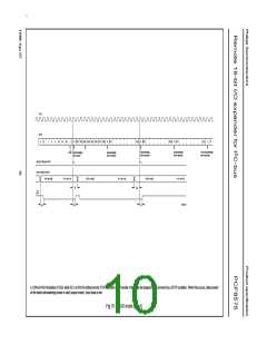
7.4
Writing to the port (output mode)
To write, the master (microcontroller) first addresses the
slave device. By setting the last bit of the byte containing
the slave address to logic 0 the write mode is entered.
The PCF8575 acknowledges and the master sends the
first data byte for P07 to P00. After the first data byte is
acknowledged by the PCF8575, the second data byte
P17 to P10 is sent by the master. Once again the
PCF8575 acknowledges the receipt of the data after which
this 16-bit data is presented on the port lines.
In the write mode the interrupt may become deactivated
(HIGH) on the rising edge of the write to port pulse. On the
falling edge of the write to port pulse the interrupt is
definitely deactivated (HIGH).
The interrupt is reset in the read mode on the rising edge
of the read from port pulse.
During the resetting of the interrupt itself any changes on
the I/Os may not generate an interrupt. After the interrupt
is reset any change in I/Os will be detected and transmitted
as an INT.
The number of data bytes that can be sent successively is
not limited. After every two bytes the previous data is
overwritten.
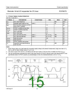
The first data byte in every pair refers to Port 0
(P07 to P00), whereas the second data byte in every pair
refers to Port 1 (P17 to P10), see Fig.11.
First Byte
Second Byte
handbook, full pagewidth
07 06 05 04 03 02 01 00
A
17 16 15 14 13 12 11 10
A
P07 P06 P05 P04 P03 P02 P01 P00
P17 P16 P15 P14 P13 P12 P11 P10
MGL545
Fig.11 Correlation between bits and ports.
1999 Apr 07
11

 NXP [ NXP ]