PCF8574; PCF8574A
NXP Semiconductors
Remote 8-bit I/O expander for I2C-bus with interrupt
13. Static characteristics
Table 9.
Static characteristics
VDD = 2.5 V to 6 V; VSS = 0 V; Tamb = 40 C to +85 C; unless otherwise specified.
Symbol
Parameter
Conditions
Min
Typ
Max
Unit
Supply
VDD
supply voltage
supply current
2.5
-
-
6.0
V
IDD
operating mode; VDD = 6 V; no load;
VI = VDD or VSS; fSCL = 100 kHz
40
100
A
Istb
standby current
standby mode; VDD = 6 V; no load;
VI = VDD or VSS
-
-
2.5
1.3
10
A
[1]
VPOR
power-on reset voltage
VDD = 6 V; no load; VI = VDD or VSS
2.4
V
Input SCL; input/output SDA
VIL
VIH
IOL
IL
LOW-level input voltage
HIGH-level input voltage
LOW-level output current
leakage current
0.5
-
-
-
-
-
+0.3VDD
V
0.7VDD
VDD + 0.5
V
VOL = 0.4 V
VI = VDD or VSS
VI = VSS
3
-
mA
A
pF
1
-
+1
7
Ci
input capacitance
I/Os; P0 to P7
VIL
LOW-level input voltage
HIGH-level input voltage
0.5
0.7VDD
-
-
-
-
+0.3VDD
VDD + 0.5
400
V
VIH
V
IIHL(max)
maximum allowed input current VI VDD or VI VSS
A
through protection diode
IOL
LOW-level output current
HIGH-level output current
VOL = 1 V; VDD = 5 V
VOH = VSS
10
30
-
25
-
-
mA
A
IOH
300
-
Itrt(pu)
transient boosted pull-up current HIGH during acknowledge (see
Figure 8); VOH = VSS; VDD = 2.5 V
1
mA
Ci
input capacitance
output capacitance
-
-
-
-
10
10
pF
pF
Co
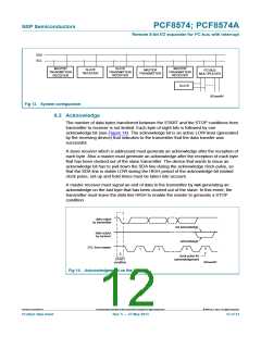
Interrupt INT (see Figure 8)
IOL LOW-level output current
IL leakage current
Select inputs A0, A1, A2
VOL = 0.4 V
1.6
-
-
-
mA
VI = VDD or VSS
1
+1
A
VIL
VIH
ILI
LOW-level input voltage
0.5
-
-
-
+0.3VDD
VDD + 0.5
+250
V
HIGH-level input voltage
input leakage current
0.7VDD
250
V
pin at VDD or VSS
nA
[1] The power-on reset circuit resets the I2C-bus logic at VDD < VPOR and sets all I/Os to logic 1 (with current source to VDD).
PCF8574_PCF8574A
All information provided in this document is subject to legal disclaimers.
© NXP B.V. 2013. All rights reserved.
Product data sheet
Rev. 5 — 27 May 2013
16 of 33

 NXP [ NXP ]