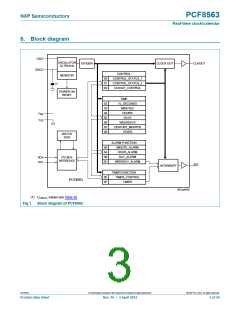
PCF8563
NXP Semiconductors
Real-time clock/calendar
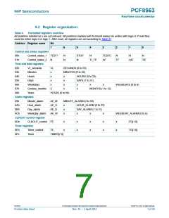
8.2 Register organization
Table 4.
Formatted registers overview
Bit positions labelled as x are not relevant. Bit positions labelled with N should always be written with logic 0; if read they
could be either logic 0 or logic 1. After reset, all registers are set according to Table 27.
Address Register name
Bit
7
6
5
4
3
2
1
0
Control and status registers
00h
01h
Control_status_1 TEST1
N
N
STOP
N
N
TESTC
AF
N
N
N
Control_status_2
N
TI_TP
TF
AIE
TIE
Time and date registers
02h
03h
04h
05h
06h
07h
08h
VL_seconds
Minutes
VL
x
SECONDS (0 to 59)
MINUTES (0 to 59)
Hours
x
x
x
x
x
HOURS (0 to 23)
DAYS (1 to 31)
Days
x
Weekdays
Century_months
Years
x
x
x
x
x
WEEKDAYS (0 to 6)
C
MONTHS (1 to 12)
YEARS (0 to 99)
Alarm registers
09h
0Ah
0Bh
0Ch
Minute_alarm
AE_M
AE_H
AE_D
AE_W
MINUTE_ALARM (0 to 59)
Hour_alarm
x
x
x
HOUR_ALARM (0 to 23)
DAY_ALARM (1 to 31)
Day_alarm
Weekday_alarm
x
x
x
x
x
x
x
x
x
WEEKDAY_ALARM (0 to 6)
CLKOUT control register
0Dh
CLKOUT_control FE
x
x
x
x
FD[1:0]
TD[1:0]
Timer registers
0Eh
0Fh
Timer_control
Timer
TE
TIMER[7:0]
PCF8563
All information provided in this document is subject to legal disclaimers.
© NXP B.V. 2012. All rights reserved.
Product data sheet
Rev. 10 — 3 April 2012
7 of 50

 NXP [ NXP ]