PCF8563
NXP Semiconductors
Real-time clock/calendar
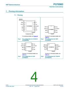
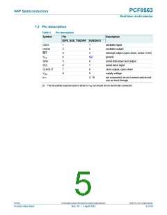
7. Pinning information
7.1 Pinning
terminal 1
index area
1
2
3
4
5
10
9
OSCI
OSCO
n.c.
n.c.
V
DD
8
PCF8563BS
CLKOUT
SCL
1
2
3
4
8
7
6
5
OSCI
OSCO
INT
V
DD
7
INT
CLKOUT
SCL
PCF8563P
6
V
SS
SDA
V
SS
SDA
001aaf981
Transparent top view
For mechanical details, see Figure 30.
001aaf977
Top view. For mechanical details, see
Figure 31.
Fig 2. Pin configuration for HVSON10
(PCF8563BS)
Fig 3. Pin configuration for DIP8
(PCF8563P)
1
2
3
4
8
7
6
5
OSCI
OSCO
INT
V
DD
1
2
3
4
8
7
6
5
OSCI
OSCO
INT
V
DD
CLKOUT
SCL
CLKOUT
SCL
PCF8563T
PCF8563TS
V
SDA
SS
V
SS
SDA
001aaf975
001aaf976
Top view. For mechanical details, see
Figure 32.
Top view. For mechanical details, see
Figure 33.
Fig 4. Pin configuration for SO8
(PCF8563T)
Fig 5. Pin configuration for TSSOP8
(PCF8563TS)
PCF8563
All information provided in this document is subject to legal disclaimers.
© NXP B.V. 2012. All rights reserved.
Product data sheet
Rev. 10 — 3 April 2012
4 of 50

 NXP [ NXP ]