Philips Semiconductors
Product specification
Single-chip 8-bit microcontroller
80C552/83C552
V
V
V
V
DD
DD
DD
DD
I
I
DD
DD
P1.6
P1.7
P1.6
P1.7
V
V
DD
P0
DD
V
V
DD
RST
V
DD
DD
STADC
P0
RST
EA
STADC
EW
EW
EA
(NC)
CLOCK SIGNAL
XTAL2
XTAL1
(NC)
CLOCK SIGNAL
XTAL2
XTAL1
AV
AV
SS
SS
V
V
SS
SS
AV
ref–
AV
ref–
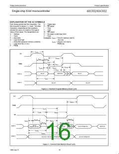
Figure 12. I Test Condition, Active Mode
Figure 13. I Test Condition, Idle Mode
DD
DD
1
2
All other pins are disconnected
All other pins are disconnected
V
V
DD
DD
I
DD
P1.6
P1.7
RST
V
DD
P0
V
DD
V
–0.5
DD
0.5V
STADC
0.7V
DD
–0.1
0.2V
DD
t
CHCX
t
t
CHCL
t
CLCX
CLCH
EW
EA
(NC)
XTAL2
XTAL1
t
CLCL
AV
SS
V
SS
AV
ref–
Figure 14. Clock Signal Waveform for I Tests in Active
Figure 15. I Test Condition, Power Down Mode
DD
All other pins are disconnected. V = 2V to 5.5V
DD
DD
3
and Idle Modes t
= t
= 5ns
CLCH
CHCL
NOTES:
1. Active Mode:
a. The following pins must be forced to V : EA, RST, Port 0, and EW.
DD
b. The following pins must be forced to V : STADC, AV , and AV .
ref–
SS
ss
c. Ports 1.6 and 1.7 should be connected to V through resistors of sufficiently high value such that the sink current into these pins cannot
DD
exceed the I
spec of these pins.
OL1
d. The following pins must be disconnected: XTAL2 and all pins not specified above.
2. Idle Mode:
a. The following pins must be forced to V : Port 0 and EW.
DD
b. The following pins must be forced to V : RST, STADC, AV ,, AV , and EA.
SS
ss
ref–
c. Ports 1.6 and 1.7 should be connected to V through resistors of sufficiently high value such that the sink current into these pins cannot
DD
exceed the I
spec of these pins. These pins must not have logic 0 written to them prior to this measurement.
OL1
d. The following pins must be disconnected: XTAL2 and all pins not specified above.
3. Power Down Mode:
a. The following pins must be forced to V : Port 0 and EW.
DD
b. The following pins must be forced to V : RST, STADC, XTAL1, AV ,, AV , and EA.
SS
ss
ref–
c. Ports 1.6 and 1.7 should be connected to V through resistors of sufficiently high value such that the sink current into these pins cannot
DD
exceed the I
spec of these pins. These pins must not have logic 0 written to them prior to this measurement.
OL1
d. The following pins must be disconnected: XTAL2 and all pins not specified above.
2
2
Purchase of Philips I C components conveys a license under the Philips’ I C patent
2
to use the components in the I C system provided the system conforms to the
I C specifications defined by Philips. This specification can be ordered using the
2
code 9398 393 40011.
20
1998 Aug 13

 NXP [ NXP ]