NTAG213F/216F
NXP Semiconductors
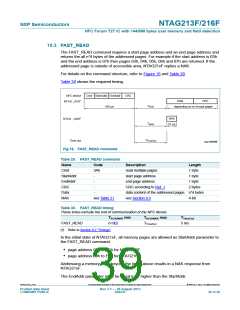
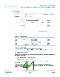
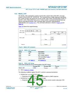
10.4 WRITE
NFC Forum T2T IC with 144/888 bytes user memory and field detection
The WRITE command requires a block address, and writes 4 bytes of data into the
addressed NTAG21xF page. The WRITE command is shown in Figure 17 and Table 31.
Table 32 shows the required timing.
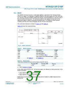
NFC device Cmd Addr
NTAG ,,ACK''
Data
CRC
ACK
T
T
ACK
NAK
708 µs
57 µs
NTAG ,,NAK''
NAK
57 µs
T
TimeOut
Time out
aaa-006990
Fig 17. WRITE command
Table 31. WRITE command
Name
Cmd
Addr
CRC
Data
NAK
Code
Description
Length
A2h
write one page
page address
CRC according to Ref. 1
data
1 byte
1 byte
2 bytes
4 bytes
4-bit
-
-
-
see Table 21
see Section 9.3
Table 32. WRITE timing
These times exclude the end of communication of the NFC device.
TACK/NAK min
n=9[1]
TACK/NAK max
TTimeOut
10 ms
WRITE
TTimeOut
[1] Refer to Section 9.2 “Timings”.
In the initial state of NTAG21xF, the following memory pages are valid Addr parameters to
the WRITE command.
• page address 02h to 2Ch for NTAG213F
• page address 02h to E6h for NTAG216F
Addressing a memory page beyond the limits above results in a NAK response from
NTAG21xF.
Pages which are locked against writing cannot be reprogrammed using any write
command. The locking mechanisms include static and dynamic lock bits as well as the
locking of the configuration pages.
NTAG213F_216F
All information provided in this document is subject to legal disclaimers.
© NXP B.V. 2013. All rights reserved.
Product data sheet
COMPANY PUBLIC
Rev. 3.1 — 28 August 2013
262231
41 of 56

 NXP [ NXP ]