Philips Semiconductors
Product specification
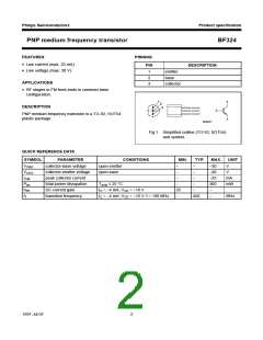
PNP medium frequency transistor
BF324
LIMITING VALUES
In accordance with the Absolute Maximum Rating System (IEC 134).
SYMBOL
PARAMETER
collector-base voltage
collector-emitter voltage
emitter-base voltage
CONDITIONS
open emitter
MIN.
MAX.
−30
UNIT
VCBO
VCEO
VEBO
IC
−
−
−
−
−
−
V
V
V
open base
−30
−4
open collector
collector current (DC)
peak collector current
total power dissipation
storage temperature
−25
−25
300
+150
150
+150
mA
mA
mW
°C
ICM
Ptot
Tamb ≤ 25 °C; note 1
Tstg
Tj
−65
−
junction temperature
°C
Tamb
operating ambient temperature
−65
°C
Note
1. Transistor mounted on an FR4 printed-circuit board.
THERMAL CHARACTERISTICS
SYMBOL
PARAMETER
CONDITIONS
VALUE
UNIT
Rth j-a
thermal resistance from junction to ambient note 1
420
K/W
Note
1. Transistor mounted on an FR4 printed-circuit board.
CHARACTERISTICS
Tj = 25 °C unless otherwise specified.
SYMBOL
PARAMETER
collector cut-off current
emitter cut-off current
DC current gain
CONDITIONS
IE = 0; VCB = −30 V
MIN.
TYP.
MAX.
UNIT
nA
ICBO
IEBO
hFE
−
−
−
−
−50
IC = 0; VEB = −4 V
VCE = −10 V
−100
nA
IC = −1 mA
−
45
−
IC = −4 mA
25
−
−
−
VBE
Crb
fT
base-emitter voltage
feedback capacitance
transition frequency
IC = −4 mA; VCE = −10 V
IC = 0; VCE = −10 V; f = 1 MHz
VCE = −10 V; f = 100 MHz
IC = −1 mA
760
−
mV
pF
−
−
0.3
−
350
450
440
−
−
−
MHz
MHz
MHz
IC = −4 mA
400
−
IC = −8 mA
1997 Jul 07
3

 NXP [ NXP ]