Philips Semiconductors
Product data
Single wire CAN transceiver
AU5790
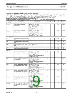
Dynamic (AC) CHARACTERISTICS for 33 kbps operation
–40 °C < T
< +125 °C; 5.5 V < V
< 16 V; –0.3 V < V
< 5.5 V; –0.3 V < V
< 5.5 V; –0.3 V < V < 5.5 V; –0.3 V < V < 5.5 V;
RxD
amb
BAT
TxD
NSTB
EN
–1 V < V
< +16 V; bus load resistor at pin RTH: 2 kΩ < R < 9.2 kΩ; total bus load resistance 270 Ω < R < 9.2 kΩ;
CANH
T
L
C < 13.7 nF; 1µs < R
C < 4µs; RxD pull-up resistor 2.2 kΩ < R < 3.0 kΩ; RxD: loaded with C < 30pF to GND;
L d LR
L
L
all voltages are referenced to pin 8 (GND); positive currents flow into the IC;
typical values reflect the approximate average value at V = 13 V and T
= 25 °C, unless otherwise specified.
amb
BAT
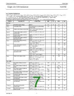
SYMBOL
PARAMETER
CONDITIONS
MIN.
TYP.
MAX.
UNIT
Pin CANH
V
CANH harmonic content in
normal mode
NSTB = 5 V, EN = 5 V;
70
dBµV
dBAMN
R = 270 Ω, C = 15 nF;
L
L
f
= 20 kHz, 50% duty cycle;
TxD
8 V < V < 16 V;
BAT
0.53 MHz < f < 1.7 MHz, Note 2
V
CANH harmonic content in
wake-up mode
NSTB = 5 V, EN = 0 V;
80
dBµV
dBAMW
R = 270 Ω, C = 15 nF;
L
L
f
= 20 kHz, 50% duty cycle;
TxD
8 V < V < 16 V;
BAT
0.53 MHz < f < 1.7 MHz, Note 2
Pins NSTB, EN
t
t
t
Normal mode to high-speed mode
delay
30
30
30
µs
µs
µs
NH
HN
WN
High-speed mode to normal mode
delay
Wake-up mode to normal mode
delay
8 V < V
< 16 V
BAT
t
t
Normal mode to sleep mode delay
Sleep mode to normal mode delay
500
50
µs
µs
NS
SN
Pin TxD
t
t
t
t
t
t
Transmit delay in normal mode,
bus rising edge
NSTB = 5 V, EN = 5 V;
3
3
3
3
3
3
6.3
µs
µs
µs
µs
µs
µs
TrN
R = 270 Ω, C = 15 nF;
L
L
5.5 V < V
< 27 V;
BAT
measured from the falling edge on
TxD to V = 3.0 V
CANH
Transmit delay in normal mode,
bus falling edge
NSTB = 5 V, EN = 5 V;
9
TfN
R = 270 Ω, C = 15 nF;
L
L
5.5 V < V
< 27 V;
BAT
measured from the rising edge on
TxD to V = 1.0 V
CANH
Transmit delay in wake-up mode,
bus rising edge to normal levels
NSTB = 0 V, EN = 5 V;
6.3
18
TrW
R = 270 Ω, C = 15 nF;
L
L
5.5 V < V
< 27 V;
BAT
measured from the falling edge on
TxD to V = 3.0 V
CANH
Transmit delay in wake-up mode,
bus rising edge to wake-up level
NSTB = 0 V, EN = 5 V;
TrW-S
TfW-3.6
TfW-4.0
R = 270 Ω, C = 15 nF;
L
L
11.3 V < V
< 27 V;
BAT
measured from the falling edge on
TxD to V = 8.9 V
CANH
Transmit delay in wake-up mode,
bus falling edge with 3.6 µs time
constant
NSTB = 0 V, EN = 5 V;
12.7
13.7
R = 270 Ω, C = 13.3 nF;
L
L
5.5 V < V
< 27 V;
BAT
measured from the rising edge on
TxD to V = 1 V, Note 2
CANH
Transmit delay in wake-up mode,
bus falling edge with 4.0 µs time
constant
NSTB = 0 V, EN = 5 V;
R = 270 Ω, C = 15 nF;
L
L
5.5 V < V
< 27 V;
BAT
measured from the rising edge on
TxD to V = 1 V
CANH
9
2001 May 18

 NXP [ NXP ]