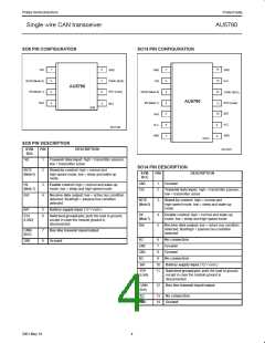
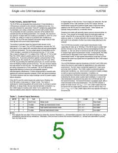
Philips Semiconductors
Product data
Single wire CAN transceiver
AU5790
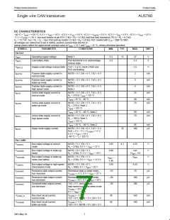
SYMBOL
PARAMETER
CONDITIONS
MIN.
TYP.
MAX.
UNIT
Pin CANH (continued)
–I
CANHH
Bus short circuit current in
high-speed mode
V
= –1 V,
50
190
mA
CANH
TxD = 0 V; NSTB = 5 V; EN = 0 V;
8 V < V
< 16 V
BAT
I
Bus leakage current at loss of
ground
(I_CAN_LG = I_CANH + I_RTH)
0 V < V
< 16 V;
–50
50
µA
CANLG
BAT
see Figure 3 in the test circuits
section
T
T
Thermal shutdown
Note 2
Note 2
155
5
190
15
°C
°C
V
sd
Thermal shutdown hysteresis
Bus input threshold
hys
V
V
V
V
5.8 V < V
all modes except sleep mode
< 27 V,
BAT
1.8
2.2
T
Bus input threshold, low battery
5.5 V < V < 5.8 V,
1.5
2.2
8.1
V
V
TL
TS
TSL
BAT
all modes except sleep mode
Bus input threshold in sleep mode NSTB = 0 V, EN = 0 V,
> 11.3 V
6.15
V
BAT
Bus input threshold in sleep mode,
low battery
NSTB = 0 V, EN = 0 V,
5.5 V < V
V
– 4.3
V
– 3.25
V
BAT
BAT
< 11.3 V
BAT
Pin RTH
V
RTH1
V
RTH2
Voltage on switched ground pin
Voltage on switched ground pin
I
I
= 1 mA
= 6 mA
0.1
1
V
V
RTH
RTH
Pins NSTB, EN
V
V
High level input voltage
Low level input voltage
Input current
5.5 V < V
5.5 V < V
< 27 V
< 27 V
3
V
V
ih
il
BAT
BAT
1
I
i
V = 1 V and V = 5 V
i
15
50
µA
i
Pin TxD
V
itxd
TxD input threshold
5.5 V < V
< 27 V
BAT
1
3
V
–I
TxD low level input current in
normal mode
NSTB = 5 V, EN = 5 V, V
= 0 V
= 5 V
50
180
µA
iltxd
TxD
TxD
–I
ihtxd
TxD high level input current in
sleep mode
NSTB = 0 V, EN = 0 V, V
–5
10
µA
Pin RxD
V
olrxd
RxD low level output voltage
I
= 2.2 mA;
0.45
V
RxD
V
V
V
= 10 V, all modes
CANH
I
I
RxD low level output current
RxD high level leakage
= 5 V; V
= 10 V
3
35
mA
olrxd
RxD
RxD
CANH
CANH
= 5 V; V
= 0 V,
–10
+10
µA
ohrxd
all modes
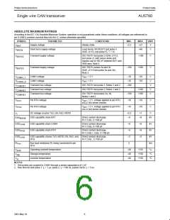
NOTES:
1. Operation at battery voltages down to 5.3 volts is guaranteed by design. Operation higher than 18 volts (18 V < V
< 27 V) for up to two
BAT
minutes is permitted if the thermal design of the board prevents reaching the thermal protection temperature limit, T , otherwise the device
sd
will self protect. Typically these requirements will be encountered during jump start operation at T
85 °C and V
< 27 V. Refer to the
amb
BAT
“Thermal Characteristics” section of this data sheet, or application note AN2005 for guidance.
2. This parameter is characterized but not subject to production test.
8
2001 May 18

 NXP [ NXP ]