Philips Semiconductors
Product specification
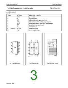
8-bit shift register with input flip-flops
74HC/HCT597
FEATURES
GENERAL DESCRIPTION
• 8-bit parallel storage register inputs
• Shift register has direct overriding load and clear
• Output capability: standard
The 74HC/HCT597 are high-speed Si-gate CMOS devices
and are pin compatible with low power Schottky TTL
(LSTTL). They are specified in compliance with JEDEC
standard no. 7A.
• ICC category: MSI
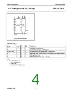
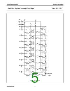
The 74HC/HCT597 consist each of an 8-bit storage
register feeding a parallel-in, serial-out 8-bit shift register.
Both the storage register and the shift register have
positive edge-triggered clocks. The shift register also has
direct load (from storage) and clear inputs.
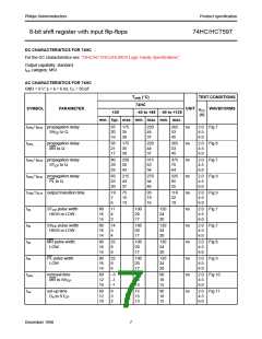
QUICK REFERENCE DATA
GND = 0 V; Tamb = 25 °C; tr = tf = 6 ns
TYPICAL
SYMBOL
PARAMETER
propagation delay
CONDITIONS
UNIT
HC
HCT
tPHL/ tPLH
CL = 15 pF; VCC = 5 V
SHCP to Q
17
25
21
96
20
ns
STCP to Q
29
26
83
3.5
32
ns
PL to Q
ns
fmax
CI
maximum clock frequency SHCP
input capacitance
MHz
pF
3.5
29
CPD
power dissipation capacitance per package notes 1 and 2
pF
Notes
1. CPD is used to determine the dynamic power dissipation (PD in µW):
2
PD = CPD × VCC2 × fi + ∑ (CL × VCC × fo) where:
fi = input frequency in MHz
fo = output frequency in MHz
2
∑ (CL × VCC × fo) = sum of outputs
CL = output load capacitance in pF
V
CC = supply voltage in V
2. For HC the condition is VI = GND to VCC
For HCT the condition is VI = GND to VCC − 1.5 V
ORDERING INFORMATION
See “74HC/HCT/HCU/HCMOS Logic Package Information”.
December 1990
2

 NXP [ NXP ]