Philips Semiconductors
Product specification
8-channel analog multiplexer/demultiplexer
74HC/HCT4051
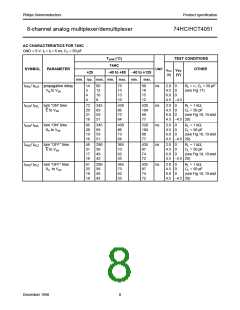
ADDITIONAL AC CHARACTERISTICS FOR 74HC/HCT
Recommended conditions and typical values
GND = 0 V; Tamb = 25 °C
VCC
(V)
VEE
(V)
Vis(p−p)
(V)
SYMBOL PARAMETER
sine-wave distortion
typ. UNIT
CONDITIONS
0.04
%
%
2.25
4.5
−2.25
−4.5
4.0
8.0
RL = 10 kΩ; CL = 50 pF
(see Fig.14)
f = 1 kHz
0.02
sine-wave distortion
f = 10 kHz
0.12
0.06
%
%
2.25
4.5
−2.25
−4.5
4.0
8.0
RL = 10 kΩ; CL = 50 pF
(see Fig.14)
switch “OFF” signal
feed-through
−50
−50
dB
dB
2.25
4.5
−2.25
−4.5
RL = 600 Ω; CL = 50 pF
(see Figs 12 and 15)
note 1
RL = 600 Ω; CL = 50 pF;
f = 1 MHz (E or Sn,
square-wave between
VCC and GND,
crosstalk voltage between
control and any switch
(peak-to-peak value)
110
220
mV
mV
4.5
4.5
0
−4.5
V(p−p)
tr = tf = 6 ns)
(see Fig.16)
minimum frequency
response (−3dB)
170
180
MHz 2.25
MHz 4.5
−2.25
−4.5
RL = 50 Ω; CL = 10 pF
(see Fig.13 and 14)
fmax
CS
note 2
maximum switch capacitance
independent (Y)
5
25
pF
pF
common
(Z)
Notes to AC characteristics
1. Adjust input voltage Vis to 0 dBm level (0 dBm = 1 mW into 600 Ω).
2. Adjust input voltage Vis to 0 dBm level at Vos for 1 MHz (0 dBm = 1 mW into 50 Ω).
General note
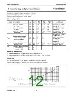
Vis is the input voltage at a Yn or Z terminal, whichever is assigned as an input.
Vos is the output voltage at a Yn or Z terminal, whichever is assigned as an output.
Test conditions:
VCC = 4.5 V; GND = 0 V; VEE = −4.5 V;
RL = 50 Ω; Rsource = 1 kΩ
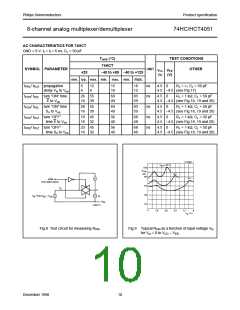
Fig.12 Typical switch “OFF” signal feed-through as a function of frequency.
December 1990
12

 NXP [ NXP ]