74HC4051-Q100; 74HCT4051-Q100
NXP Semiconductors
8-channel analog multiplexer/demultiplexer
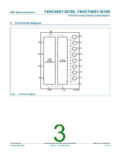
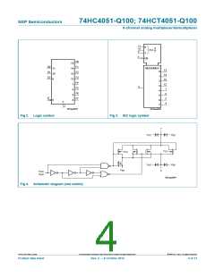
7. Functional description
7.1 Function table
Table 3.
Function table[1]
Input
Channel ON
E
L
L
L
L
L
L
L
L
H
S2
L
S1
L
S0
L
Y0 to Z
Y1 to Z
Y2 to Z
Y3 to Z
Y4 to Z
Y5 to Z
Y6 to Z
Y7 to Z
switches off
L
L
H
L
L
H
H
L
L
H
L
H
H
H
H
X
L
H
L
H
H
X
H
X
[1] H = HIGH voltage level;
L = LOW voltage level;
X = don’t care.
8. Limiting values
Table 4.
Limiting values
In accordance with the Absolute Maximum Rating System (IEC 60134). Voltages are referenced to VSS = 0 V (ground).
Symbol
VCC
IIK
Parameter
Conditions
Min
Max
+11.0
20
20
25
20
50
Unit
V
[1]
supply voltage
0.5
input clamping current
VI < 0.5 V or VI > VCC + 0.5 V
-
mA
mA
mA
mA
mA
mA
C
ISK
switch clamping current VSW < 0.5 V or VSW > VCC + 0.5 V
-
ISW
IEE
switch current
0.5 V < VSW < VCC + 0.5 V
-
supply current
-
ICC
supply current
-
IGND
Tstg
Ptot
P
ground current
-
50
+150
500
100
storage temperature
total power dissipation
power dissipation
65
[2]
-
-
mW
mW
per switch
[1] To avoid drawing VCC current out of terminal Z, when switch current flows into terminals Yn, the voltage drop across the bidirectional
switch must not exceed 0.4 V. If the switch current flows into terminal Z, no VCC current will flow out of terminals Yn, and in this case
there is no limit for the voltage drop across the switch, but the voltages at Yn and Z may not exceed VCC or VEE
.
[2] For SO16 packages: above 70 C the value of Ptot derates linearly with 8 mW/K.
For TSSOP16 package: above 60 C the value of Ptot derates linearly with 5.5 mW/K.
For DHVQFN16 packages: above 60 C the value of Ptot derates linearly with 4.5 mW/K.
74HC_HCT4051_Q100
All information provided in this document is subject to legal disclaimers.
© NXP B.V. 2012. All rights reserved.
Product data sheet
Rev. 2 — 8 October 2012
6 of 31

 NXP [ NXP ]